LTC1334 Ver la hoja de datos (PDF) - Linear Technology
Número de pieza
componentes Descripción
Lista de partido
LTC1334 Datasheet PDF : 16 Pages
| |||
LTC1334
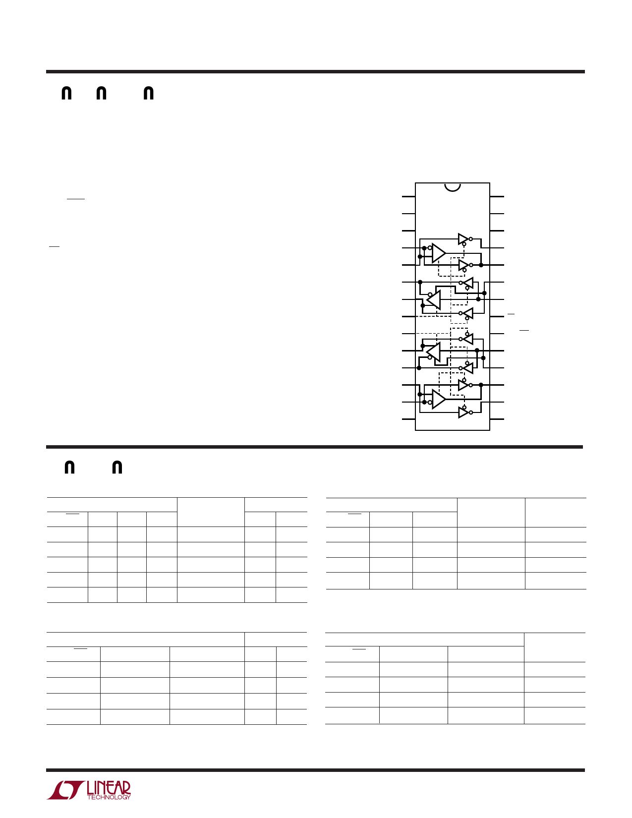
PI FU CTIO S
RB2 (Pin 16): Receiver Output.
RA2 (Pin 17): Receiver Output.
DZ2/DE2 (Pin 18): RS232 Driver Input in RS232 Mode.
RS485 Driver Enable with internal pull-up in RS485 mode.
DY2 (Pin 19): Driver Input.
ON/OFF (Pin 20): A high logic input enables the transceiv-
ers. A low puts the device into shutdown mode and
reduces ICC to 10µA. This pin has an internal pull-up.
LB (Pin 21): Loopback Control Input. A low logic level
enables internal loopback connections. This pin has an
internal pull-up.
DY1 (Pin 22): Driver Input.
DZ1/DE1 (Pin 23): RS232 Driver Input in RS232 Mode.
RS485 Driver Enable with internal pull-up in RS485 mode.
RA1 (Pin 24): Receiver Output.
RB1 (Pin 25): Receiver Output.
VCC (Pin 26): Positive Supply; 4.75V ≤ VCC ≤ 5.25V
C2– (Pin 27): Commutating Capacitor C2 Negative Termi-
nal. Requires 0.1µF external capacitor between Pins 27
and 28.
C2+ (Pin 28): Commutating Capacitor C2 Positive Terminal.
C1+ 1
C1– 2
VDD 3
4
A1
B1 5
Y1 6
7
Z1
SEL1 8
SEL2 9
10
Z2
11
Y2
B2 12
13
A2
GND 14
28 C2+
27 C2–
26
VCC
25
RB1
24
RA1
23
DZ1/DE1
22
DY1
21
LB
20
ON/OFF
19
DY2
18 DZ2/DE2
17
RA2
16
RB2
15 VEE
UU
FU CTIO TABLES
RS485 Driver Mode
RS232 Driver Mode
INPUTS
ON/OFF SEL DE D
CONDITIONS
OUTPUTS
Z
Y
INPUTS
ON/OFF SEL
D
CONDITIONS
OUTPUTS
Y, Z
1
1
10
No Fault
0
1
1
0
0
No Fault
1
1
1
11
No Fault
1
0
1
0
1
No Fault
0
1
1
1 X Thermal Fault
Z
Z
1
0
X
Thermal Fault
Z
1
1
0X
X
Z
Z
0
0
X
X
Z
0
1
XX
X
Z
Z
RS485 Receiver Mode
ON/OFF
INPUTS
SEL
B–A
1
1
< – 0.2V
1
1
> 0.2V
1
1
Inputs Open
0
1
X
*See Note 5 of Electrical Characteristics table.
OUTPUTS
RA
RB*
0
1
1
1
1
1
Z
Z
RS232 Receiver Mode
ON/OFF
INPUTS
SEL
1
0
1
0
1
0
0
0
A, B
0
1
Inputs Open
X
OUTPUTS
RA, RB
1
0
1
Z
7
Share Link: 