LTC1705 Ver la hoja de datos (PDF) - Linear Technology
Número de pieza
componentes Descripción
Lista de partido
LTC1705
Linear Technology

LTC1705 Datasheet PDF : 28 Pages
| |||
LTC1705
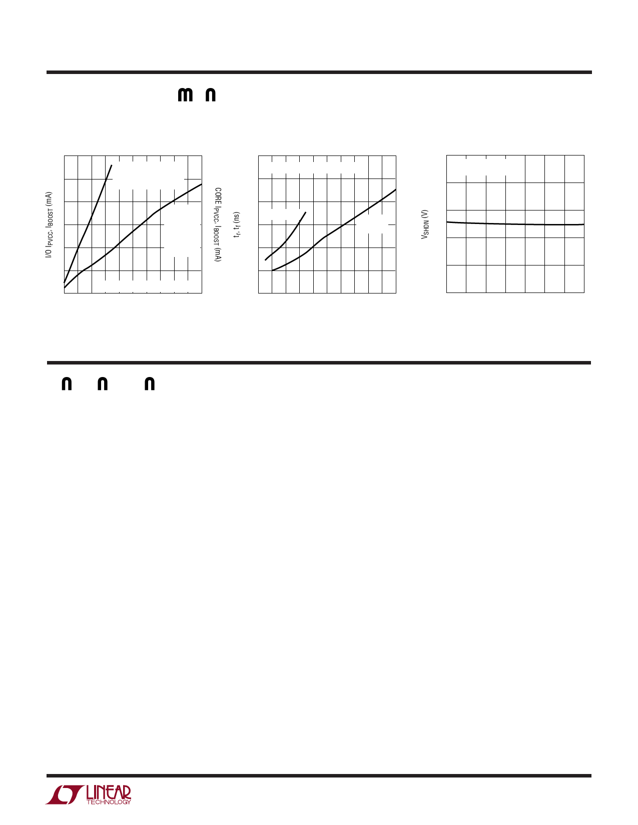
TYPICAL PERFOR A CE CHARACTERISTICS
IPVCC, IBOOST vs Driver Load
12
36
I/O DRIVERS
10
SUPPLY CURRENT
WITH CORE DISABLED
30
8
24
CORE
DRIVERS
6
SUPPLY 18
CURRENT
4
WITH I/O
DISABLED
12
2
6
TA = 25°C, PVCC = BOOST = 5V
0
0
0 2000 4000 6000 8000 10000
TG, BG LOAD (pF)
1705 G26
Drivers Rise and Fall Time vs
Load
60
TA = 25°C, PVCC = BOOST = 5V
50
40
I/O DRIVERS
30
20
CORE
DRIVERS
10
0
0 2000 4000 6000 8000 10000
TG, BG LOAD (pF)
1705 G27
VSHDN vs Temperature
0.80
VCC = 5V
MEASURED AT RUN/SS
0.68
0.56
0.44
0.32
0.20
–50 –25
0 25 50 75
TEMPERATURE (°C)
100 125
1705 G28
PI FU CTIO S
IMAXIO (Pin 1): I/O Supply Current Limit Set. The IMAXIO pin
sets the current limit comparator threshold for the I/O
controller. If the voltage drop across the bottom MOSFET,
QBIO, exceeds the magnitude of the voltage at IMAXIO, the
I/O controller enters current limit. The IMAXIO pin has an
internal 10µA current source pull-up, allowing the current
threshold to be set with a single external resistor to PGND.
Kelvin connect this current setting resistor to the source of
QBIO. Refer to the Current Limit Programming section for
more information on choosing the value of RIMAX.
PVCC (Pin 2): Driver Power Supply Input. PVCC provides
power to the BGC and BGIO output drivers. PVCC must be
connected to a voltage high enough to fully turn on the
external MOSFETs QBC and QBIO. PVCC should generally
be connected directly to VIN, the main system 5V supply.
PVCC requires at least a 10µF bypass capacitor directly to
PGND.
BOOSTC (Pin 3): Core Controller Top Gate Driver Supply.
The BOOSTC pin supplies power to the floating TGC driver.
Bypass BOOSTC to SWC with a 1µF capacitor. An external
schottky diode from VIN to BOOSTC creates a complete
floating charge-pumped supply at BOOSTC. No other
external supplies are required.
BGC (Pin 4): Core Supply Bottom Gate Drive. The BGC pin
drives the gate of the bottom N-channel synchronous
switch MOSFET, QBC. BGC is designed to typically drive
up to 10,000pF of gate capacitance. If RUN/SS goes low,
BGC goes low, turning off QBC.
TGC (Pin 5): Core Supply Top Gate Drive. The TGC pin
drives the gate of the top N-channel MOSFET, QTC. The
TGC driver draws power from the BOOSTC pin and returns
it to the SWC pin, providing true floating drive to QTC. TGC
is designed to typically drive up to 10,000pF of gate
capacitance. If RUN/SS goes low, TGC goes low, turning
off QTC.
SWC (Pin 6): Core Supply Switching Node. Connect SWC
to the switching node of the core converter. The TGC driver
ground returns to SWC, providing floating gate drive to the
top N-channel MOSFET switch, QTC. The voltage at SWC
is compared to IMAXC by the current limit comparator while
the bottom MOSFET, QBC, is on.
PGND (Pin 7): Power Ground. The BGC and BGIO drivers
return to this pin. Connect PGND to a high-current ground
node in close proximity to the sources of external MOSFETs
QBC and QBIO, and the VIN and VOUT bypass capacitors.
IMAXC (Pin 8): Core Supply Current Limit Set. See IMAXIO.
7
Share Link: