LTC2209IUP Ver la hoja de datos (PDF) - Linear Technology
Número de pieza
componentes Descripción
Lista de partido
LTC2209IUP Datasheet PDF : 32 Pages
| |||
Features
n Sample Rate: 160Msps
n 77.3dBFS Noise Floor
n 100dB SFDR
n SFDR >84dB at 250MHz (1.5VP-P Input Range)
n PGA Front End (2.25VP-P or 1.5VP-P Input Range)
n 700MHz Full Power Bandwidth S/H
n Optional Internal Dither
n Optional Data Output Randomizer
n LVDS or CMOS Outputs
n Single 3.3V Supply
n Power Dissipation: 1.53W
n Clock Duty Cycle Stabilizer
n Pin-Compatible Family:
130Msps: LTC2208 (16-Bit), LTC2208-14 (14-Bit)
105Msps: LTC2217 (16-Bit)
n 64-Pin (9mm × 9mm) QFN Package
Applications
n Telecommunications
n Receivers
n Cellular Base Stations
n Spectrum Analysis
n Imaging Systems
n ATE
LTC2209
16-Bit, 160Msps ADC
Description
The LTC®2209 is a 160Msps 16-bit A/D converter designed
for digitizing high frequency, wide dynamic range signals
with input frequencies up to 700MHz. The input range of
the ADC can be optimized with the PGA front end.
The LTC2209 is perfect for demanding communications
applications, with AC performance that includes 77.3dBFS
Noise Floor and 100dB spurious free dynamic range
(SFDR). Ultra low jitter of 70fsRMS allows undersampling
of high input frequencies with excellent noise performance.
Maximum DC specs include ±5.5LSB INL, ±1LSB DNL (no
missing codes).
The digital output can be either differential LVDS or
single-ended CMOS. There are two format options for
the CMOS outputs: a single bus running at the full data
rate or demultiplexed busses running at half data rate. A
separate output power supply allows the CMOS output
swing to range from 0.5V to 3.6V.
The ENC+ and ENC– inputs may be driven differentially
or single-ended with a sine wave, PECL, LVDS, TTL or
CMOS inputs. An optional clock duty cycle stabilizer al-
lows high performance at full speed with a wide range of
clock duty cycles.
L, LT, LTC and LTM are registered trademarks of Linear Technology Corporation.
All other trademarks are the property of their respective owners.
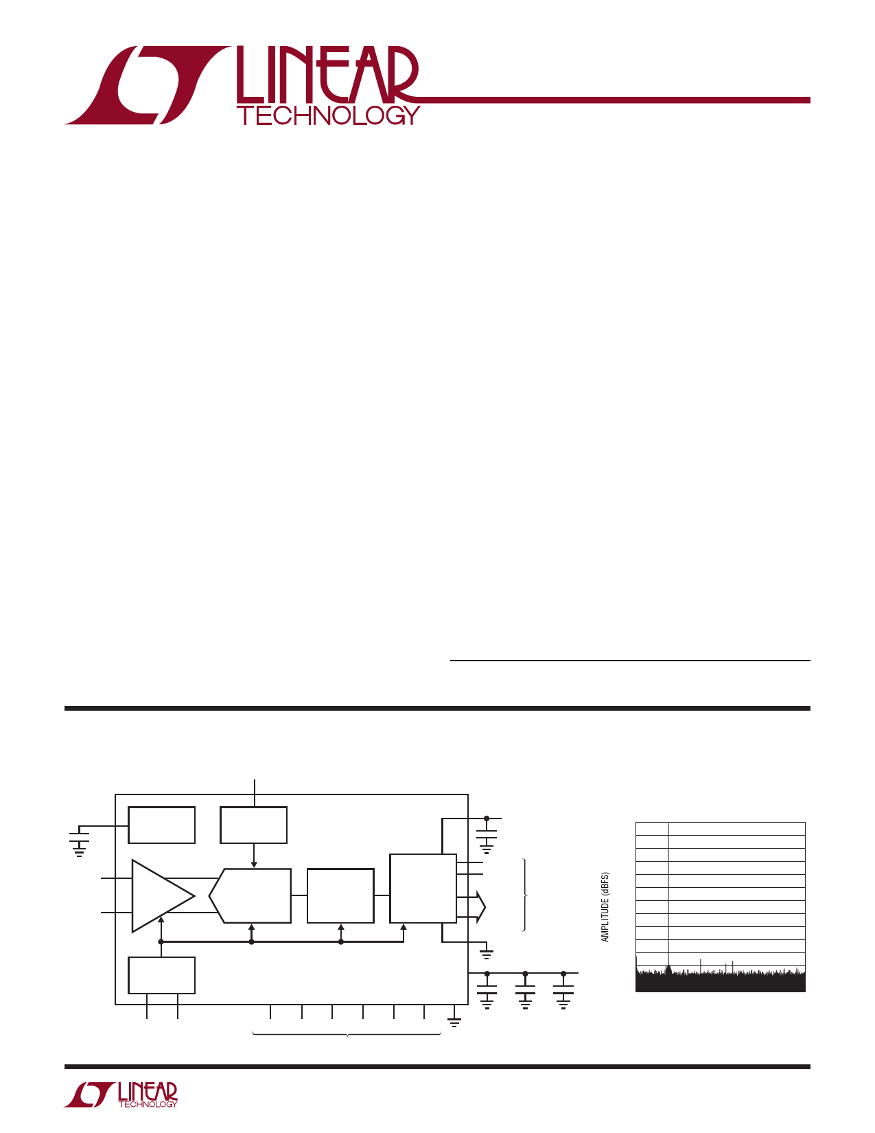
Typical Application
VCM
2.2µF
1.25V
COMMON MODE
BIAS VOLTAGE
AIN +
ANALOG
INPUT
AIN –
+
S/H
AMP
–
CLOCK/DUTY
CYCLE
CONTROL
ENC + ENC –
3.3V
SENSE
INTERNAL ADC
REFERENCE
GENERATOR
OVDD
16-BIT
PIPELINED
ADC CORE
CORRECTION
LOGIC AND
SHIFT REGISTER
OUTPUT
DRIVERS
OGND
VDD
GND
PGA SHDN DITH MODE LVDS RAND
ADC CONTROL INPUTS
0.5V TO 3.6V
1µF
OF
CLKOUT
D15
•
•
•
D0
CMOS
OR
LVDS
1µF
1µF
3.3V
1µF
2209 TA01
64k Point FFT, fIN = 15.1MHz,
–1dBFS, PGA = 0
0
–10
–20
–30
–40
–50
–60
–70
–80
–90
–100
–110
–120
–130
0
10 20 30 40 50 60 70 80
FREQUENCY (MHz)
2209 TA01b
2209fb
1
Share Link: 