LTC3544EUD-TRPBF Ver la hoja de datos (PDF) - Linear Technology
Número de pieza
componentes Descripción
Lista de partido
LTC3544EUD-TRPBF
Linear Technology

LTC3544EUD-TRPBF Datasheet PDF : 16 Pages
| |||
LTC3544
OPERATION (Refer to Functional Diagrams)
The LTC3544 uses a constant-frequency current mode
architecture. The operating frequency is set at 2.25MHz.
All channels share the same clock and run in-phase.
The output voltage for each regulator is set by an external
resistor divider returned to the VFB pin. An error ampli-
fier compares the divided output voltage with a reference
voltage of 0.8V and regulates the peak inductor current
accordingly.
Main Control Loop
During normal operation, the top power switch (P-channel
MOSFET) is turned on at the beginning of a clock cycle
when the VFB voltage is below the reference voltage. The
current into the inductor and the load increases until the
peak inductor current (controlled by ITH) is reached. The RS
latch turns off the top switch, turns on the bottom switch,
and energy stored in the inductor is discharged through
the bottom switch (N-channel MOSFET) into the load until
the next clock cycle begins, or until the inductor current
begins to reverse (sensed by the IRCMP comparator).
The peak inductor current is controlled by the internally
compensated ITH voltage, which is the output of the er-
ror amplifier. This amplifier regulates the VFB pin to the
internal 0.8V reference by adjusting the peak inductor
current accordingly.
Burst Mode Operation
To optimize efficiency, the LTC3544 automatically switches
from continuous operation to Burst Mode operation when
the load current is relatively light. During Burst Mode
operation, the peak inductor current (as set by ITH) re-
mains fixed at a low level and the PMOS switch operates
intermittently based on load demand. By running cycles
periodically, the switching losses are minimized.
The duration of each burst event can range from a few
cycles at light load to almost continuous cycling with
short sleep intervals at moderate loads. During the sleep
intervals, the load current is being supplied solely from
the output capacitor. As the output voltage droops, the
error amplifier output rises above the sleep threshold,
signaling the burst comparator to trip and turn the top
MOSFET on. This cycle repeats at a rate that is dependent
on load demand.
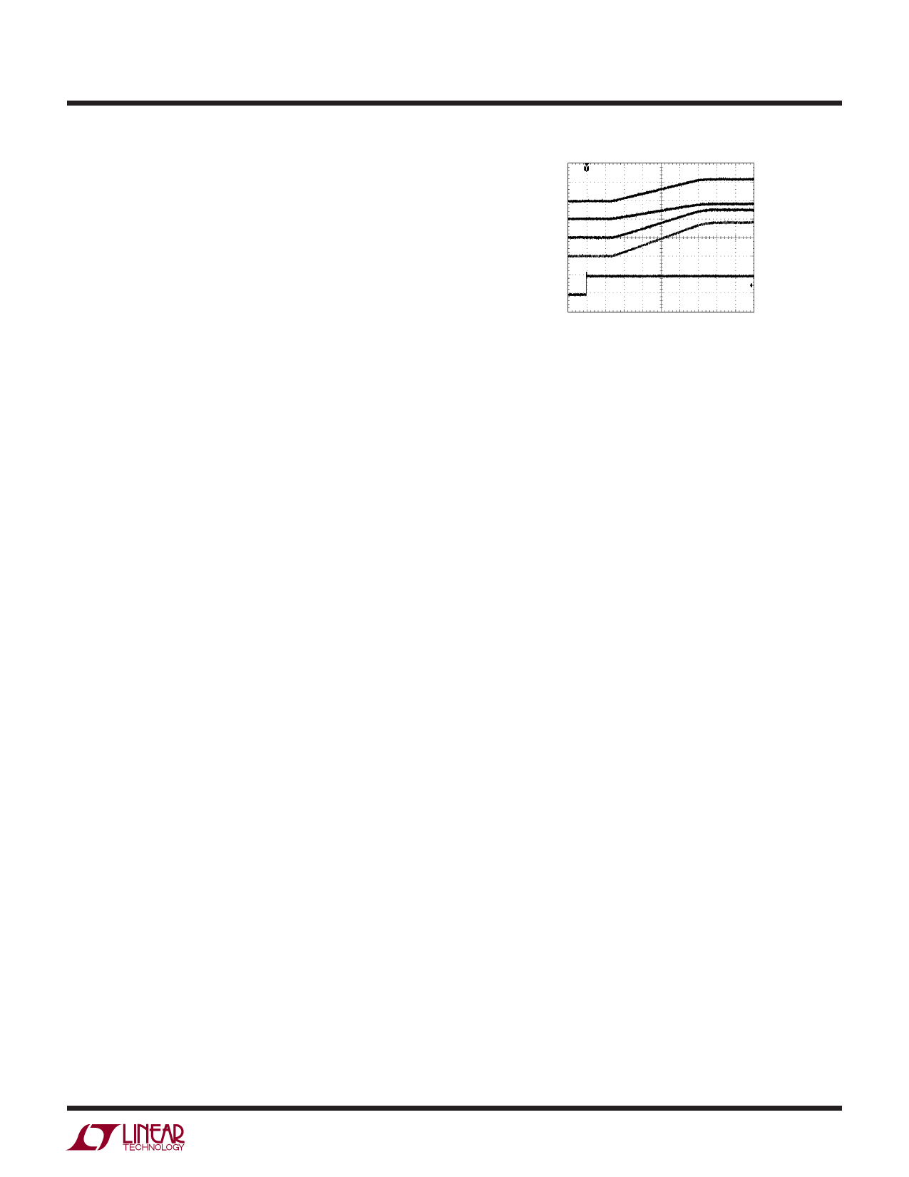
VOUT100
VOUT200A
VOUT200B
VOUT300
RUNx
VIN = 3.6V
200μs/DIV
TA = 25°C
ALL CHANNELS UNLOADED
3544 G12
Figure 1. Regulator Soft-Start
Soft-Start
Soft-start reduces surge currents on VIN and output
overshoot during start-up. Soft-start on the LTC3544 is
implemented by internally ramping the reference signal
fed to the error amplifier over approximately a 1ms period.
Figure 1 shows the behavior of the four regulator channels
during soft-start.
Short-Circuit Protection
Short-circuit protection is achieved by monitoring the in-
ductor current. When the current exceeds a predetermined
level, the main switch is turned off, and the synchronous
switch is turned on long enough to allow the current in the
inductor to decay below the fault threshold. This prevents
a catastrophic inductor current, run-away condition, but
will still provide current to the output. Output voltage
regulation in this condition is not achieved.
DROPOUT OPERATION
As the input supply voltage decreases to a value approach-
ing the output voltage, the duty cycle increases toward the
maximum on-time. Further reduction of the supply voltage
forces the main switch to remain on for more than one cycle
until it reaches 100% duty cycle. The output voltage will
then be determined by the input voltage minus the voltage
drop across the P-channel MOSFET and the inductor. An
important detail to remember is that at low input supply
voltages, the RDS(ON) of the P-channel switch increases
(see Typical Performance Characteristics). Therefore,
the user should calculate the power dissipation when
the LTC3544 is used at 100% duty cycle with low input
voltage (see Thermal Considerations in the Applications
Information section).
3544fa
9
Share Link: