LX5225CDWP Ver la hoja de datos (PDF) - Microsemi Corporation
Número de pieza
componentes Descripción
Lista de partido
LX5225CDWP Datasheet PDF : 4 Pages
| |||
LX5225
PRODUCT DATABOOK 1996/1997
ULTRA 18-LINE, PLUG AND PL AY SCSI TERMINATOR
PRODUCTION DATA SHEET
UltraMAX
A B S O L U T E M A X I M U M R AT I N G S (Note 1)
TermPwr Voltage ................................................................................................. +7V
Signal Line Voltage ................................................................................... 0V to +7V
Operating Junction Temperature
Plastic (DWP Packages) ............................................................................... 150°C
Storage Temperature Range .............................................................. -65°C to 150°C
Lead Temperature (Soldering, 10 seconds) .................................................... 300°C
Note 1. Exceeding these ratings could cause damage to the device. All voltages are with
respect to Ground. Currents are positive into, negative out of the specified
terminal.
T H E R MAL DATA
DWP PACKAGE:
THERMAL RESISTANCE-JUNCTION TO LEADS, θJL
18°C/W
THERMAL RESISTANCE-JUNCTION TO AMBIENT, θJA
40°C/W
Junction Temperature Calculation: TJ = TA + (PD x θJA).
The θJA numbers are guidelines for the thermal performance of the device/pc-board
system. All of the above assume no ambient airflow.
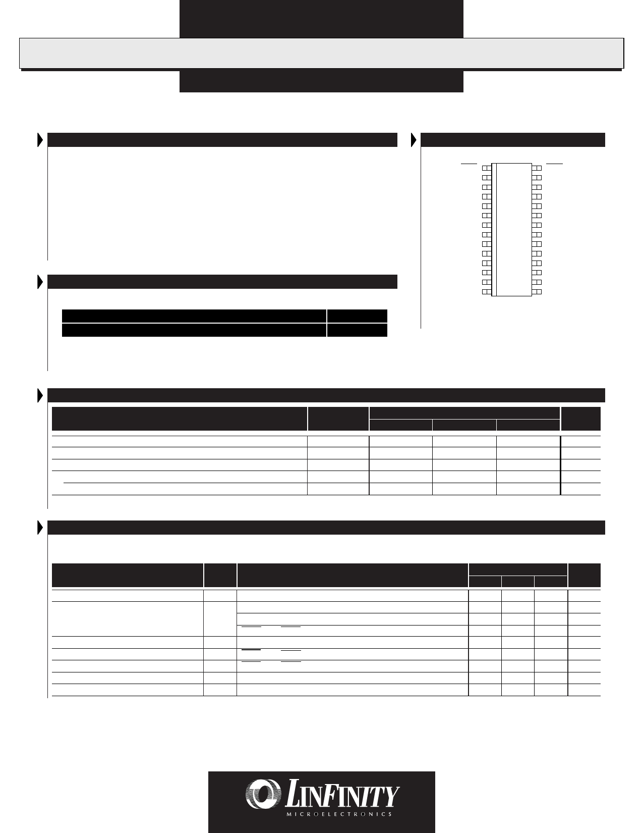
PACKAGE PIN OUTS
DISC1
T1
T2
T3
T4
T5
HEAT SINK/GND
GND
HEAT SINK/GND
T6
T7
T8
T9
VTERM
1
28
2
27
3
26
4
25
5
24
6
23
7
22
8
21
9
20
10
19
11
18
12
17
13
16
14
15
DISC2
T18
T17
T16
T15
T14
HEAT SINK/GND
HEAT SINK/GND
HEAT SINK/GND
T13
T12
T11
T10
N.C.
DWP PACKAGE
(Top View)
R E C O M M E N D E D O P E R AT I N G C O N D I T I O N S (Note 2)
Parameter
Symbol
Recommended Operating Conditions
Min.
Typ.
Max.
Termpwr Voltage
Signal Line Voltage
VTERM
4.0
5.5
0
5
Disconnect Input Voltage
Operating Virtual Junction Temperature Range
0
VTERM
LX5225C
0
125
Note 2. Range over which the device is functional.
Units
V
V
V
°C
ELECTRICAL CHARACTERISTICS
Term Power = 4.75V unless otherwise specified. Unless otherwise specified, these specifications apply at the recommended operating ambient tempera-
ture of T = 25°C. Low duty cycle pulse testing techniques are used which maintains junction and case temperatures equal to the ambient temperature.
A
Parameter
Symbol
Test Conditions
LX5225
Units
Min. Typ. Max.
Output High Voltage
TermPwr Supply Current
VOUT
ICC All data lines = open
All data lines = 0.2V
2.65 2.85
V
10
15
mA
424 450 mA
DISC1 and DISC2 Pins < 0.8V
50 150 µA
Output Current
Disconnect Input Current
Output Leakage Current
Channel Bandwidth
IOUT VOUT = 0.2V
IIN DISC1 and DISC2 Pins = 0V
IOL DISC1 and DISC2 Pins = < 0.8V, VO = 0.2V
BW
-20 -22 -24 mA
-10
µA
1
µA
35
MHz
Termination Sink Current, per Channel
ISINK
VOUT = 4V
7
mA
2
Copyright © 1999
Rev. 1.0 5/99
Share Link: 