LT1237CG Ver la hoja de datos (PDF) - Linear Technology
Número de pieza
componentes Descripción
Lista de partido
LT1237CG
Linear Technology

LT1237CG Datasheet PDF : 8 Pages
| |||
LT1237
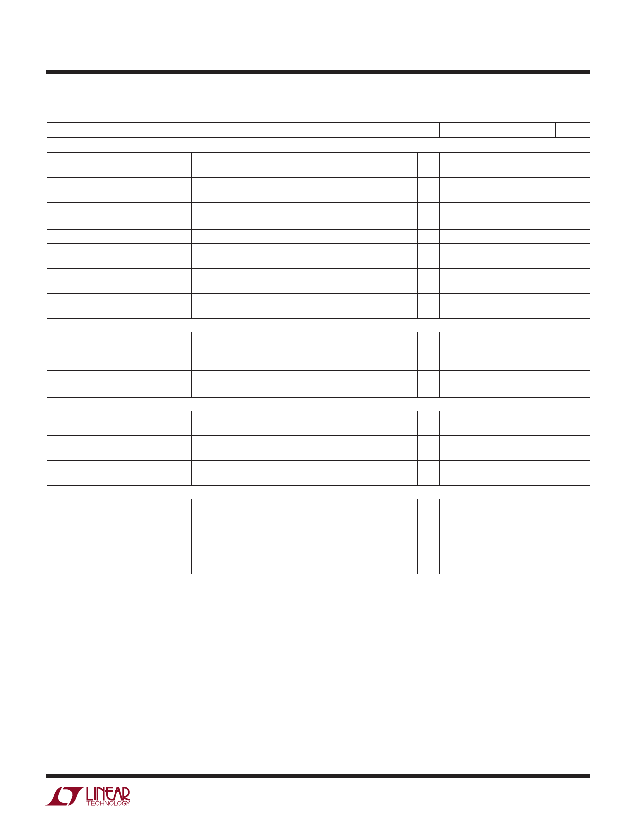
ELECTRICAL CHARACTERISTICS The q denotes specifications which apply over the full operating
temperature range, otherwise specifications are at TA = 25°C. (Note 2)
PARAMETER
Any Driver
Output Voltage Swing
Logic Input Voltage Level
Logic Input Current
Output Short-Circuit Current
Output Leakage Current
Data Rate (Note 7)
Slew Rate
Propagation Delay
Any Receiver
Input Voltage Thresholds
Hysteresis
Input Resistance
Output Leakage Current
Receivers 1, 2, 3, 4
Output Voltage
Output Short-Circuit Current
Propagation Delay
Receiver 5 (LOW ISUPPLY RX)
Output Voltage
Output Short-Circuit Current
Propagation Delay
CONDITIONS
Load = 3k to GND
Positive
Negative
Input Low Level (VOUT = High)
Input High Level (VOUT = Low)
0.8V ≤ VIN ≤ 2V
VOUT = 0V
Shutdown VOUT = ±30V (Note 4)
RL = 3k, CL = 2500pF
RL = 3k, CL = 1000pF
RL = 3k, CL = 51pF
RL = 3k, CL = 2500pF
Output Transition tHL High to Low (Note 5)
Output Transition tLH Low to High
Input Low Threshold (VOUT = High)
Input High Threshold (VOUT = Low)
VIN = ±10V
Shutdown (Note 4) 0 ≤ VOUT ≤ VCC
Output Low, IOUT = – 1.6mA
Output High, IOUT = 160µA (VCC = 5V)
Sinking Current, VOUT = VCC
Sourcing Current, VOUT = 0V
Output Transition tHL High to Low (Note 6)
Output Transition tLH Low to High
Output Low, IOUT = – 500µA
Output High, IOUT = 160µA (VCC = 5V)
Sinking Current, VOUT = VCC
Sourcing Current, VOUT = 0V
Output Transition tHL High to Low (Note 6)
Output Transition tLH Low to High
MIN TYP MAX
q
5.0
7.5
q
– 6.3 – 5.0
q
1.4
0.8
q 2.0
1.4
q
5
20
±9
17
q
10
100
120
250
15
30
4
7
0.6
1.3
0.5
1.3
0.8
1.3
1.7
2.4
q 0.1
0.4
1.0
3
5
7
q
1
10
q
0.2
0.4
q 3.5
4.2
– 10 – 20
10
20
250 600
350 600
q
0.2
0.4
q 3.5
4.2
–2
–4
2
4
1.0
3
0.6
3
UNITS
V
V
V
V
µA
mA
µA
kBaud
kBaud
V/µs
V/ µs
µs
µs
V
V
V
kΩ
µA
V
V
mA
mA
ns
ns
V
V
mA
mA
µs
µs
Note 1: Absolute Maximum Ratings are those values beyond which the life
of the device may be impaired.
Note 2: Testing done at VCC = 5V and VON/OFF = 3V, unless otherwise
specified.
Note 3: Supply current is measured as the average over several charge
pump burst cycles. C+ = 1.0µF, C – = 0.1µF, C1 = C2 = 0.2µF. All outputs
are open, with all driver inputs tied high.
Note 4: Measurements in shutdown are performed with VON/OFF ≤ 0.1V.
Supply current measurements using driver disable are performed with
VDRIVER DISABLE ≥ 3V.
Note 5: For driver delay measurements, RL = 3k and CL = 51pF. Trigger
points are set between the driver’s input logic threshold and the output
transition to the zero crossing (tHL = 1.4V to 0V and tLH = 1.4V to 0V).
Note 6: For receiver delay measurements, CL = 51pF. Trigger points are
set between the receiver’s input logic threshold and the output transition
to standard TTL/CMOS logic threshold (tHL = 1.3V to 2.4V and tLH = 1.7V
to 0.8V).
Note 7: Data rate operation guaranteed by slew rate, short-circuit current
and propagation delay tests.
3
Share Link: