LT1237CSW Ver la hoja de datos (PDF) - Linear Technology
Número de pieza
componentes Descripción
Lista de partido
LT1237CSW
Linear Technology

LT1237CSW Datasheet PDF : 8 Pages
| |||
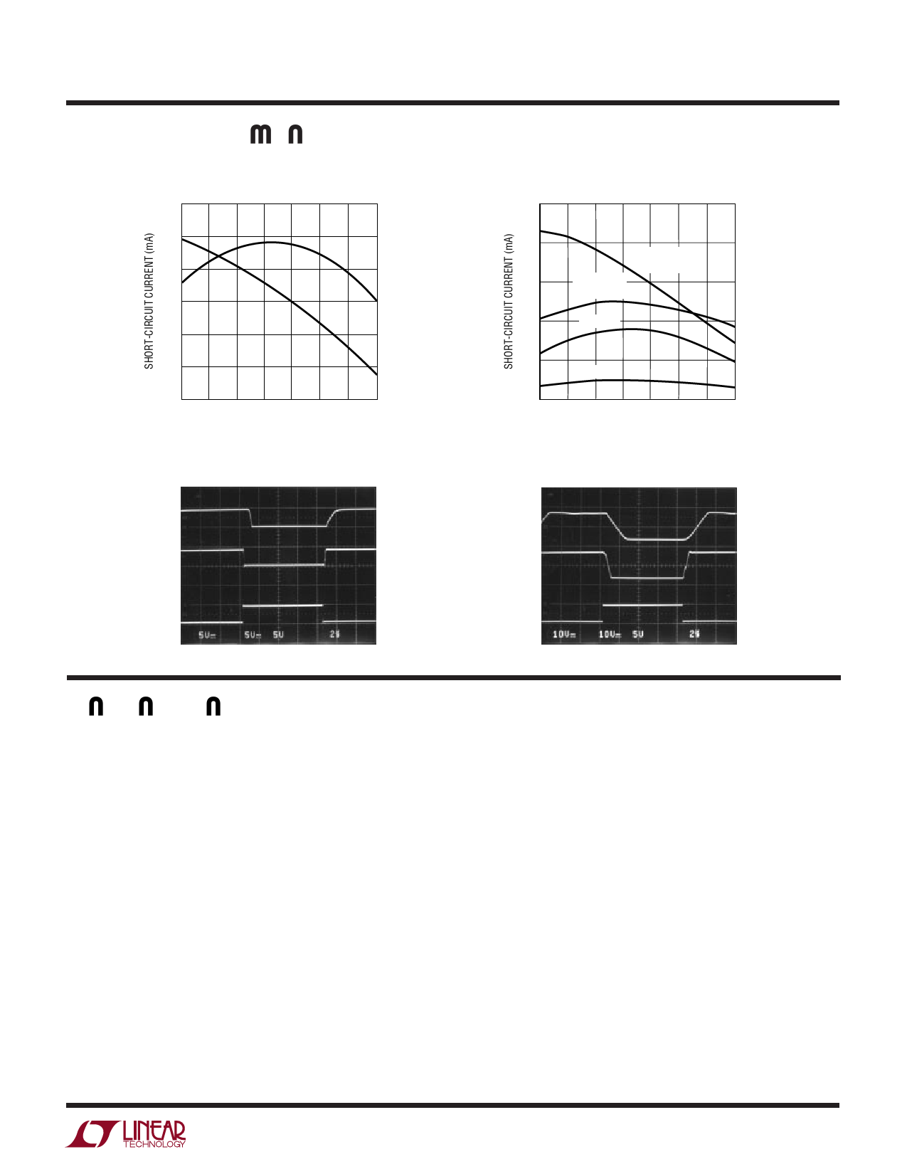
TYPICAL PERFOR A CE CHARACTERISTICS
LT1237
Driver Short-Circuit Current
30
25
ISC+
20
15
ISC–
10
5
0
–55 –25
0 25 50 75
TEMPERATURE (°C)
100 125
1237 G10
Receiver Output Waveforms
Receiver Short-Circuit Current
50
40
RX1 TO RX4
ISC–
30
RX1 TO RX4
ISC+
20
RX5 ISC–
10
RX5 ISC+
0
–55 –25
0 25 50 75
TEMPERATURE (°C)
100 125
1237 G11
Driver Output Waveforms
RX5 OUTPUT
CL = 50pF
RX1 TO RX4
OUTPUT
CL = 50pF
INPUT
1237 G12
DRIVER OUTPUT
RL = 3k
CL = 2500pF
DRIVER OUTPUT
RL = 3k
INPUT
1237 G13
PI FU CTIO S
VCC: 5V Input Supply Pin. This pin should be decoupled
with a 0.1µF ceramic capacitor close to the package pin.
Insufficient supply bypassing can result in low output
drive levels and erratic charge pump operation.
GND: Ground Pin.
ON/OFF: TTL/CMOS Compatible Operating Mode Control.
A logic low puts the device in the low power shutdown
mode. All three drivers and four receivers (RX1, RX2, RX3,
and RX4) assume a high impedance output state in shut-
down. Only receiver RX5 remains active while the trans-
ceiver is in shutdown. The transceiver consumes only
60µA of supply current while in shutdown. A logic high
fully enables the transceiver.
DRIVER DISABLE: This pin provides an alternate control
for the charge pump and RS232 drivers. A logic high on
this pin shuts down the charge pump and places all driver
outputs in a high impedance state. All five receivers remain
active under these conditions. Floating the driver disable
pin or driving it to a logic low level fully enables the
transceiver. A logic low on the ON/OFF pin supersedes the
state of the DRIVER DISABLE pin. Supply current drops to
3mA when in driver disable mode.
V+: Positive Supply Output (RS232 Drivers). V+ ≈ 2VCC –
1.5V. This pin requires an external charge storage capaci-
tor C ≥ 1.0µF, tied to ground or VCC. Larger value capaci-
tors may be used to reduce supply ripple. The ratio of the
capacitors on V+ and V – should be greater than 5 to 1.
V–: Negative Supply Output (RS232 Drivers). V – ≈
–(2VCC – 2.5V). This pin requires an external charge
storage capacitor C ≥ 0.1µF. See the Applications Infor-
mation section for guidance in choosing filter capacitors
for V+ and V –.
5
Share Link: