MASW-007076-000100 Ver la hoja de datos (PDF) - M/A-COM Technology Solutions, Inc.
Número de pieza
componentes Descripción
Lista de partido
MASW-007076-000100
M/A-COM Technology Solutions, Inc.

MASW-007076-000100 Datasheet PDF : 4 Pages
| |||
MASW-007076-000100
GaAs SPST Absorptive Switch with
ASIC Driver, DC-3.0 GHz
Rev. V4
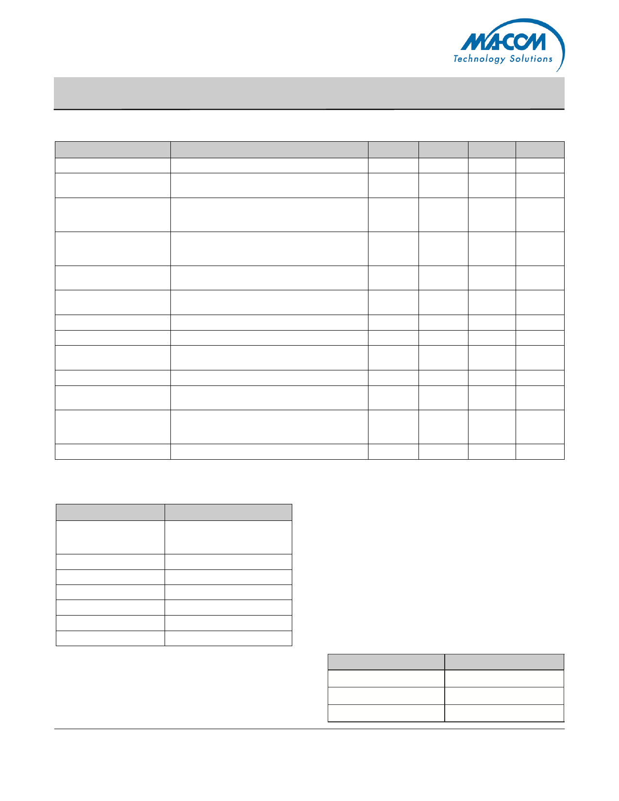
Electrical Specifications: TA = 25°C, Z0 = 50Ω
Parameter
Test Conditions
Units
Min
Typ
Max
Insertion Loss
DC - 3.0 GHz
dB
—
1.8
2.2
Isolation
(All arms off)
DC - 3.0 GHz
dB
35
42
—
VSWR
Trise Tfall
Ton
Toff
Transients
DC - 3.0 GHz
On
Off
10%/90%, 90%/10% 1
50% TTL to 90%/10% RF
In-band (peak to peak)
—
—
1.6:1
2.1:1
—
—
2.0:1
2.1:1
ns
—-
15
50
ns
—
50
150
mV
—
50
150
1 dB Compression
Input IP3
.05 GHz
.5 - 3.0 GHz
Two tone inputs 0.05 GHz
Up to +5 dBm 0.5 - 3.0 GHz
dBm
—
+20
—
dBm
—
+27
—
dBm
—
+35
—
dBm
—
+46
—
VCC
VEE
VIL
VIH
lin (Input Leakage Current)
Icc
(Quiescent Supply Current)
ΔIcc
(Additional Supply Current Per
TTL Input Pin)
—
—
LOW-level input voltage
HIGH-level input voltage
Vin = VCC or GND
Vcntrl = VCC or GND
VCC = Max, Vcntrl = VCC - 2.1 V
V
+4.5
+5.0
+5.5
V
-8.0
-5.0
-4.75
V
0.0
—
0.8
V
2.0
—
5.0
uA
-1.0
—
1.0
uA
—
250
400
mA
—
—
1.0
IEE
VEE min to max, Vin = VIL or VIH
mA
-1.0
-0.2
—
1. Decoupling capacitors (.01 µF) are required on the power supply lines.
Absolute Maximum Ratings 2,3
Parameter
Max. Input Power
0.05 GHz
0.5 - 3.0 GHz4
VCC
VEE
VCC - VEE
Vin5
Operating Temperature
Storage Temperature
Absolute Maximum
+27 dBm
+34 dBm
-0.5V ≤ VCC ≤ +7.0V
-8.5V ≤ VEE ≤ +0.5V
-0.5V ≤ VCC - VEE ≤ 14.5V
-0.5V ≤ Vin ≤ VCC + 0.5V
-40ºC to +85ºC
-65ºC to +125ºC
Handling Procedures
Please observe the following precautions to avoid
damage:
Static Sensitivity
Gallium Arsenide Integrated Circuits are sensitive
to electrostatic discharge (ESD) and can be
damaged by static electricity. Proper ESD control
techniques should be used when handling these
devices.
Truth Table
2. Exceeding any one or combination of these limits may cause
permanent damage to this device.
TTL Control Input
RF Common To:
3. M/A-COM does not recommend sustained operation near
these survivability limits.
C1
RF1
4. When the RF input is applied to the terminated port, the
absolute maximum power is +30 dBm.
1
On
5. Standard CMOS TTL interface, latch-up will occur if logic
signal is applied prior to power supply.
2
0
Off
ADVANCED: Data Sheets contain information regarding a product M/A-COM Technology Solutions • North America Tel: 800.366.2266 • Europe Tel: +353.21.244.6400
is considering for development. Performance is based on target specifications, simulated results,
and/or prototype measurements. Commitment to develop is not guaranteed.
PRELIMINARY: Data Sheets contain information regarding a product M/A-COM Technology
• India Tel: +91.80.4155721
• China Tel: +86.21.2407.1588
Visit www.macomtech.com for additional data sheets and product information.
Solutions has under development. Performance is based on engineering tests. Specifications are
typical. Mechanical outline has been fixed. Engineering samples and/or test data may be available. M/A-COM Technology Solutions Inc. and its affiliates reserve the right to make
Commitment to produce in volume is not guaranteed.
changes to the product(s) or information contained herein without notice.
Share Link: