L4923 Ver la hoja de datos (PDF) - STMicroelectronics
Número de pieza
componentes Descripción
Lista de partido
L4923 Datasheet PDF : 6 Pages
| |||
L4923
FUNCTIONAL DESCRIPTION
The operating principle of the voltage regulator is
basedon thereference,the error amplifier,the driver
and the power PNP. This stage uses an Isolated
CollectorVertical PNP transistor which allowsto ob-
tain very low dropout voltage (typ. 450 mV) and low
quiescent current (IQ = 20 mA typically at IO = 1 A).
Thanks to these features the device is particularly
suited when the power dissipation must be limited
as, for example, in automotive or industrial applica-
tions supplied by battery.
The three gain stages (operational amplifier, driver
and power PNP) require the external capacitor
(COmin = 22 µF) to guarantee the global stability of
the system.
The antisaturationcircuit allows to reducedrastically
the current peak which takes place during the start
up.
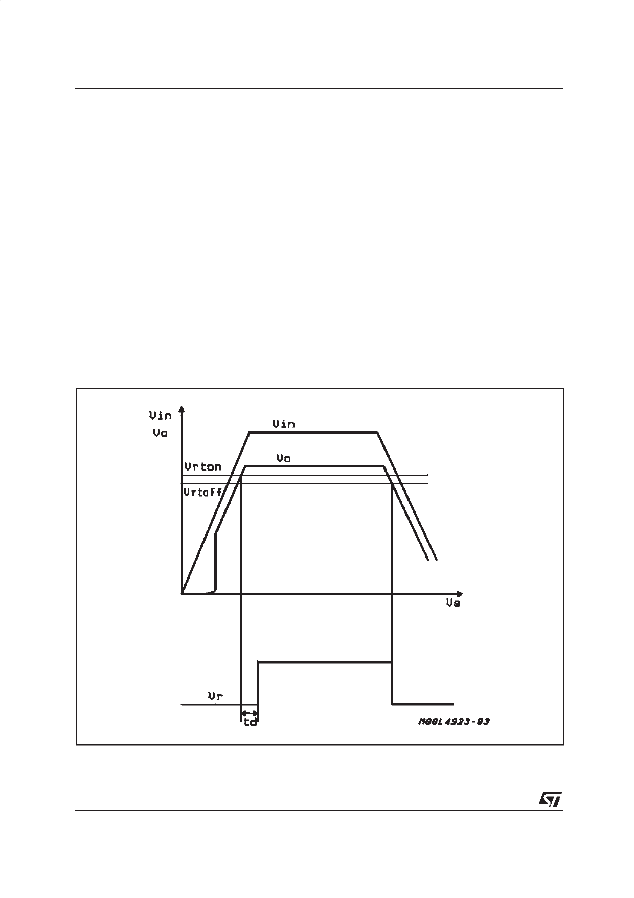
The reset function is LOW active when the output
voltage level is lower than the reset threshold volt-
age VRth (typ.value : VO - 150 mV). When the output
voltage is higher than VRth the reset becomes HIGH
aftera delay time settablewith theexternalcapacitor
Cd. Typically td = 20 ms, Cd = 0.1 µF. The reset
threshold hysteresis improves the noise immunity
allowing to avoid false switchings. The typical reset
output waveform is shown in fig. 2.
The inhibit circuit acceptsstandardTTL inputlevels :
thisblockswitchesoffthe voltageregulatorwhen the
input signal is HIGH and switches on it when the in-
put signal is LOW. Thanksto inhibit functionthe con-
sumption is drastically reduced (650 µA max) when
no load current is required.
Figure 2 : Typical Reset Output Waveform.
4/6
Share Link: 