MAX604 Ver la hoja de datos (PDF) - Maxim Integrated
Número de pieza
componentes Descripción
Lista de partido
MAX604 Datasheet PDF : 12 Pages
| |||
5V/3.3V or Adjustable, Low-Dropout,
Low IQ, 500mA Linear Regulators
_____________________________Typical Operating Characteristics (continued)
(VIN = 7V for MAX603, VIN = 5.3V for MAX604, OFF = VIN, SET = GND, CIN = COUT = 10µF, RL = 1kΩ, TJ = +25°C, unless otherwise noted.)
LOAD-TRANSIENT RESPONSE
OVERSHOOT AND TIME
EXITING SHUTDOWN MODE
B
5V
A
A
B
MAX603
VOUT = 5V
2ms/div
A: OUTPUT VOLTAGE (100mV/div)
B: IOUT = 500mA (HIGH), IOUT = 5mA (LOW)
0V
500µs/div
A: OFF PIN VOLTAGE (1V/div)
RISE TIME = 13µs
B: MAX603 OUTPUT VOLTAGE (1V/div)
DELAY = 4.936ms, OVERSHOOT = 1%, RISE TIME = 55µs
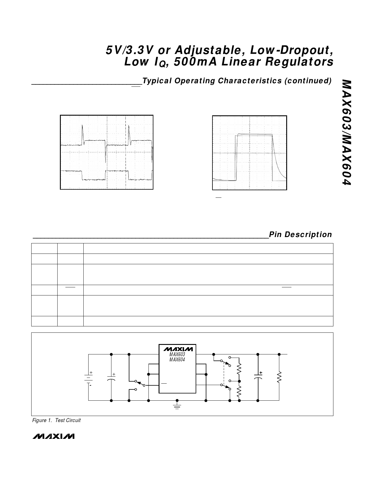
______________________________________________________________Pin Description
PIN
NAME
DESCRIPTION
1
IN Regulator Input. Supply voltage can range from 2.7V to 11.5V.
2, 3, 6, 7
GND
Ground. These pins function as heatsinks, only in the SOIC package. All GND pins must be soldered to the
circuit board for proper power dissipation. Connect to large copper pads or planes to channel heat from the IC.
4
OFF Shutdown, active low. Switch logic levels in less than 1µs with the high level above the OFF threshold.
5
SET
Feedback for Setting the Output Voltage. Connect to GND to set the output voltage to the preselected 3.3V
or 5V. Connect to an external resistor network for adjustable output operation.
8
OUT Regulator Output. Fixed or adjustable from 1.25V to 11.0V. Sources up to 500mA for input voltages above 4V.
1
IN
8
MAX603 OUT
2
MAX604
GND
GND
7
VIN
3 GND
GND 6
CIN
10µF
4
OFF
SET 5
VOUT
R1
COUT
RL
10µF
R2
Figure 1. Test Circuit
_______________________________________________________________________________________ 5
Share Link: 