MAX7432A Ver la hoja de datos (PDF) - Maxim Integrated
Número de pieza
componentes Descripción
Lista de partido
MAX7432A Datasheet PDF : 21 Pages
| |||
Standard Definition Video Reconstruction
Filters and Buffers
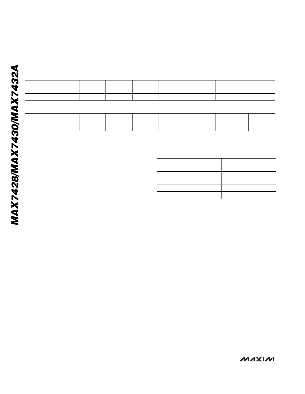
Table 3. MAX7430 Control Register
(MSB)
NAME
—
ABSEL2
BYPASS2 CLEVEL2 BOOST1(2) BOOST0(2)
OUT
DISABLE2
—
DEFAULT
0
1
1
0
0
0
0
0
NAME
—
ABSEL1 BYPASS1 CLEVEL1 BOOST1(1) BOOST0(1)
OUT
—
DISABLE1
DEFAULT
0
1
1
0
0
0
0
0
FIRST BIT
(LSB)
CLEVEL: Clamp Level bit. A logic 0 selects a clamp
level of 1V while a logic 0 selects a clamp level of 1.5V
at the output.
[BOOST1, BOOST0]: High-Frequency Boost Control bits.
The adjust bits select the amount of high-frequency boost
for the filter. Table 2 defines four levels of adjustment.
OUTDISABLE: Output Disable bit. A logic 0 selects
normal operation while a logic 1 places the output in a
high-impedance state.
MAX7430 Control Register
Table 3 defines the structure of the MAX7430 16-bit con-
trol register programmed by MSPB. This register controls
the selection of IN_A or IN_B, selection of filter 1 or 2, filter
bypassing, clamp-level selection, high-frequency boost
control, and output disable. See Maxim’s Single Pin Bus
Interface (MSPB) section for detailed programming
instructions.
ABSEL_: Channel Select bit. A logic zero selects the
input at IN_B to be processed while a logic 1 selects
the input at IN_A to be processed.
BYPASS_: Filter Bypass Select bit. A logic 1 selects
the channel filter while a logic 0 bypasses the channel
filter.
CLEVEL_: Clamp Level bit. A logic 0 selects a channel
clamp level of 1V while a logic 0 selects a channel
clamp level of 1.5V at the output.
[BOOST1_, BOOST0_]: High-Frequency Boost Control
bits. The adjust bits select the amount of high-frequency
boost for the channel filter. Table 4 defines four levels of
adjustment.
OUTDISABLE_: Output Disable bit. A logic 0 selects
normal channel output operation while a logic 1 puts
the channel output in a high-impedance state.
Table 4. Boost Level Programming
BOOST1_
0
0
1
1
BOOST0_
0
1
0
1
RELATIVE HIGH
FREQUENCY BOOST
0
0.3dB to 0.5dB
0.6dB to 1.0dB
0.9dB to 1.5dB
MAX7432A Control Register
Table 5 defines the structure of the MAX7432A 24-bit
control register programmed by MSPB. This register
controls the selection of IN_A or IN_B, selection of filter
1, 2, or 3, filter bypassing, clamp-level selection, high-
frequency boost control, and output disable. See
Maxim’s Single-Pin Bus Interface (MSPB) section for
detailed programming instructions.
ABSEL_: Channel Select bit. A logic zero selects the
input at IN_B to be processed while a logic 1 selects
the input at IN_A to be processed.
BYPASS_: Filter Bypass Select bit. A logic 1 selects
the channel filter while a logic 0 bypasses the channel
filter.
CLEVEL_: Clamp Level bit. A logic 0 selects a channel
clamp level of 1V while a logic 0 selects a channel
clamp level of 1.5V at the output.
[BOOST1_, BOOST0_]: High-Frequency Boost Control
bits. The adjust bits select the amount of high-frequency
boost for the channel filter. Table 6 defines four levels of
adjustment.
OUTDISABLE_: Output Disable Bit. A logic 0 selects
normal channel output operation while a logic 1 puts
the channel output in high-impedance state.
10 ______________________________________________________________________________________
Share Link: 