MB90860E Ver la hoja de datos (PDF) - Fujitsu
Número de pieza
componentes Descripción
Lista de partido
MB90860E Datasheet PDF : 67 Pages
| |||
MB90860E Series
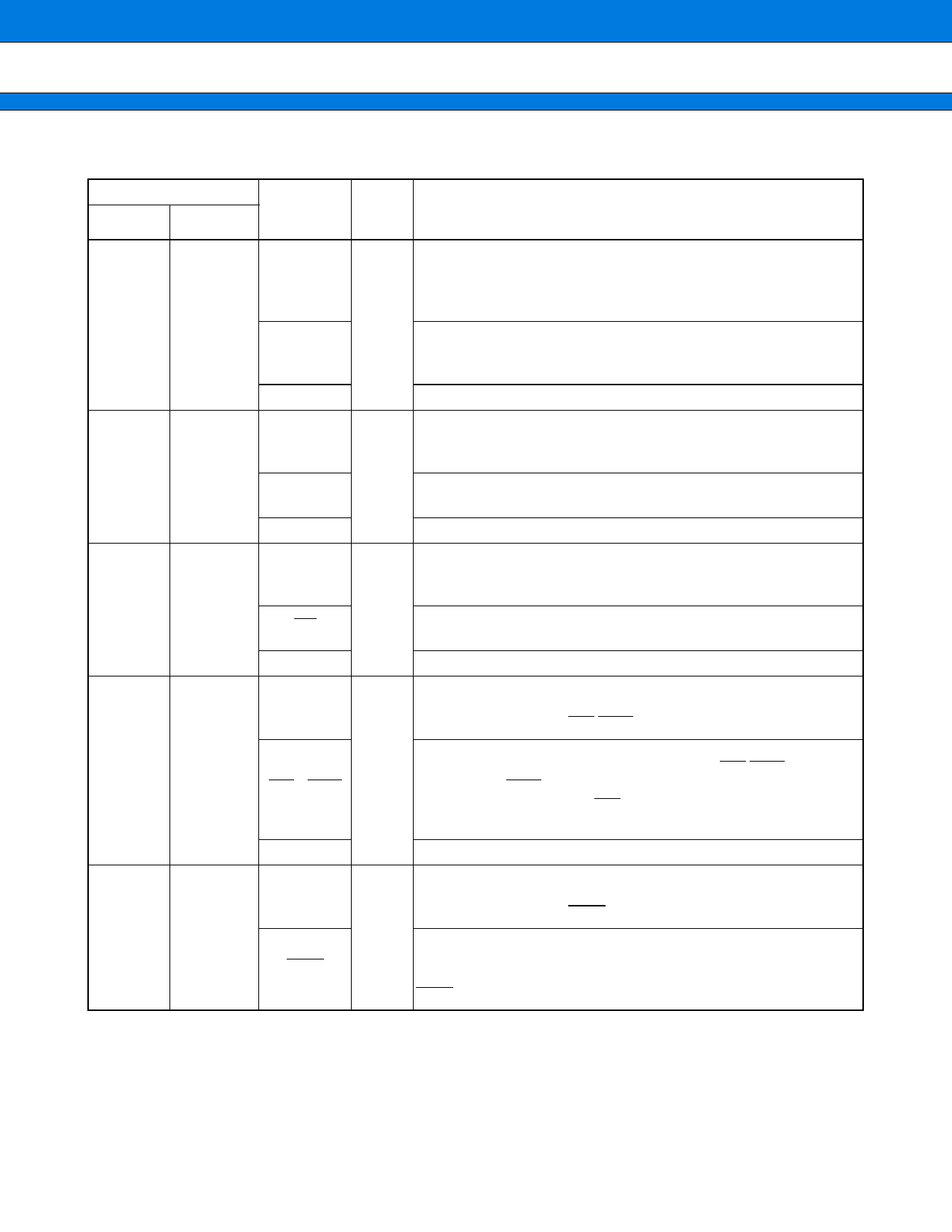
■ PIN DESCRIPTION
Pin No.
I/O
Pin name Circuit
QFP100*1 LQFP100*2
type*3
Function
1 to 4
P24 to P27
99 to 2
A20 to A23
General purpose I/O pins. The register can be set to select
whether to use a pull-up resistor.In external bus mode, the pin is
enabled as a general-purpose I/O port when the corresponding bit
in the external address output control register (HACR) is 1.
G Output pins of the external address bus. When the corresponding
bit in the external address output control register (HACR) is 0, the
pins are enabled as high address output pins (A20 to A23).
IN0 to IN3
Trigger input pins for input captures 0 to 3.
General purpose I/O pin.The register can be set to select whether
P30
to use a pull-up resistor.This function is enabled in single-chip
mode.
5
3
ALE
G Address latch enable output pin. This function is enabled when
the external bus is enabled.
IN4
Trigger input pin for input capture 4.
General purpose I/O pin.The register can be set to select whether
P31
to use a pull-up resistor.This function is enabled in single-chip
mode.
6
4
RD
G External read strobe output pin. This function is enabled when the
external bus is enabled.
IN5
Trigger input pin for input capture 5.
General purpose I/O pin. The register can be set to select whether
P32
to use a pull-up resistor. This function is enabled either in single-
chip mode or with the WR/WRL pin output disabled.
Write strobe output pin for the external data bus. This function is
7
5
G enabled when both the external bus and the WR/WRL pin output
WR / WRL
are enabled. WRL is used to write-strobe 8 lower bits of the data
bus in 16-bit access while WR is used to write-strobe 8 bits of the
data bus in 8-bit access.
INT10R
External interrupt request input pin (sub) .
General purpose I/O pin. The register can be set to select whether
P33
to use a pull-up resistor.This function is enabled either in single-
chip mode or with the WRH pin output disabled.
8
6
G Write strobe output pin for the 8 higher bits of the external data
WRH
bus. This function is enabled when the external bus is enabled,
when the external bus 16-bit mode is selected, and when the
WRH output pin is enabled.
(Continued)
10
Share Link: 