MC14541B(2000) Ver la hoja de datos (PDF) - ON Semiconductor
Número de pieza
componentes Descripción
Lista de partido
MC14541B Datasheet PDF : 8 Pages
| |||
MC14541B
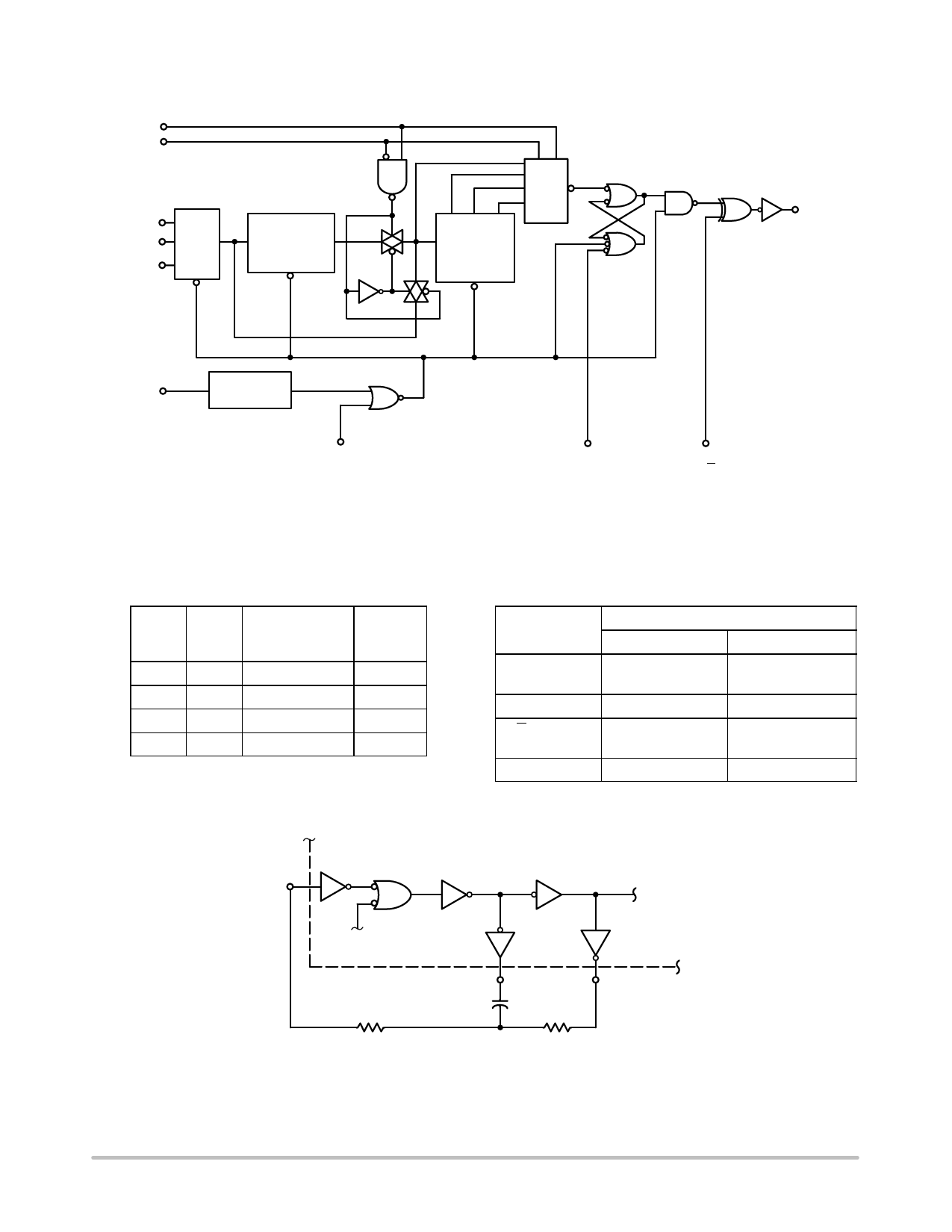
TYPICAL RC OSCILLATOR CHARACTERISTICS
8.0
VDD = 15 V
4.0
0
10 V
– 4.0
– 8.0
5.0 V
– 12
RTC = 56 kΩ,
– 16 C = 1000 pF
– 55 – 25
RS = 0, f = 10.15 kHz @ VDD = 10 V, TA = 25°C
RS = 120 kΩ, f = 7.8 kHz @ VDD = 10 V, TA = 25°C
0
25
50
75 100 125
TA, AMBIENT TEMPERATURE (°C)
Figure 4. RC Oscillator Stability
100
50
20
10
5.0
f AS A FUNCTION
2.0
OF C
1.0 (RTC = 56 kΩ)
(RS = 120 kΩ)
0.5
VDD = 10 V
f AS A FUNCTION
OF RTC
(C = 1000 pF)
(RS ≈ 2RTC)
0.2
0.1
1.0 k
0.0001
10 k
100 k
RTC, RESISTANCE (OHMS)
0.001
0.01
C, CAPACITANCE (µF)
1.0 m
0.1
Figure 5. RC Oscillator Frequency as a
Function of Rtc and Ctc
OPERATING CHARACTERISTICS
With Auto Reset pin set to a “0” the counter circuit is
initialized by turning on power. Or with power already on,
the counter circuit is reset when the Master Reset pin is set
to a “1”. Both types of reset will result in synchronously
resetting all counter stages independent of counter state.
Auto Reset pin when set to a “1” provides a low power
operation.
The RC oscillator as shown in Figure 3 will oscillate with
a frequency determined by the external RC network i.e.,
f= 1
2.3 RtcCtc
v v if (1 kHz f 100 kHz)
and RS ≈ 2 Rtc
where RS ≥ 10 kΩ
The time select inputs (A and B) provide a two–bit address
to output any one of four counter stages (28, 210, 213 and
216). The 2n counts as shown in the Frequency Selection
Table represents the Q output of the Nth stage of the counter.
When A is “1”, 216 is selected for both states of B. However,
when B is “0”, normal counting is interrupted and the 9th
counter stage receives its clock directly from the oscillator
(i.e., effectively outputting 28).
The Q/Q select output control pin provides for a choice of
output level. When the counter is in a reset condition and
Q/Q select pin is set to a “0” the Q output is a “0”,
correspondingly when Q/Q select pin is set to a “1” the Q
output is a “1”.
When the mode control pin is set to a “1”, the selected
count is continually transmitted to the output. But, with
mode pin “0” and after a reset condition the RS flip–flop (see
Expanded Block Diagram) resets, counting commences,
and after 2n–1 counts the RS flip–flop sets which causes the
output to change state. Hence, after another 2n–1 counts the
output will not change. Thus, a Master Reset pulse must be
applied or a change in the mode pin level is required to reset
the single cycle operation.
Rtc
1
Ctc
2
3
RS
NC
4
AR
5
MR
6
INPUT
7
tMR
DIGITAL TIMER APPLICATION
14
13
12
11
10 MODE
9 Q/Q
8
VDD
B
A
N.C.
VDD
OUTPUT
t + tMR
When Master Reset (MR) receives a positive pulse, the
internal counters and latch are reset. The Q output goes high
and remains high until the selected (via A and B) number of
clock pulses are counted, the Q output then goes low and
remains low until another input pulse is received.
This “one shot” is fully retriggerable and as accurate as the
input frequency. An external clock can be used (pin 3 is the
clock input, pins 1 and 2 are outputs) if additional accuracy
is needed.
Notice that a setup time equal to the desired pulse width
output is required immediately following initial power up,
during which time Q output will be high.
http://onsemi.com
5
Share Link: 