MC14553BCPG Ver la hoja de datos (PDF) - ON Semiconductor
Número de pieza
componentes Descripción
Lista de partido
MC14553BCPG Datasheet PDF : 8 Pages
| |||
MC14553B
OPERATING CHARACTERISTICS
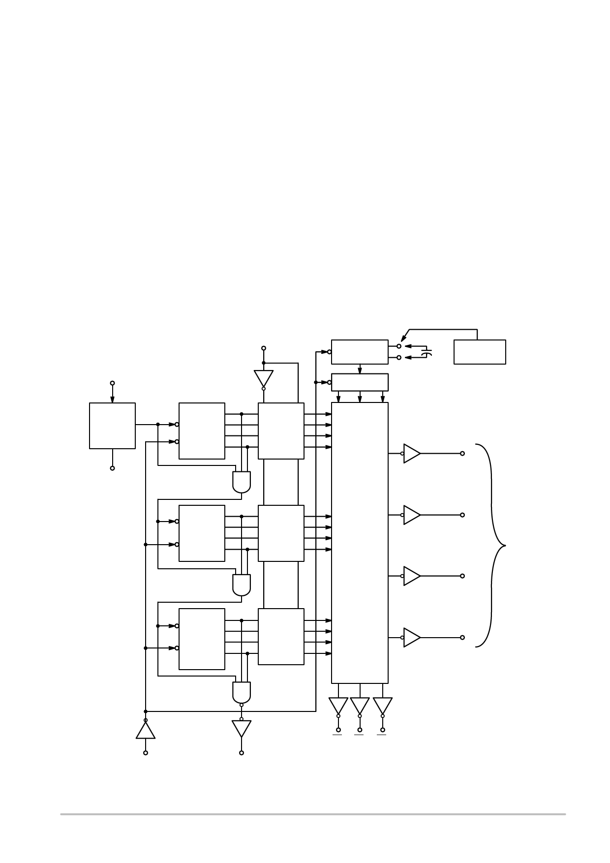
The MC14553B three−digit counter, shown in Figure 4,
consists of three negative edge−triggered BCD counters
which are cascaded in a synchronous fashion. A quad latch
at the output of each of the three BCD counters permits
storage of any given count. The three sets of BCD outputs
(active high), after going through the latches, are time
division multiplexed, providing one BCD number or digit at
a time. Digit select outputs (active low) are provided for
display control. All outputs are TTL compatible.
An on−chip oscillator provides the low frequency
scanning clock which drives the multiplexer output selector.
The frequency of the oscillator can be controlled externally
by a capacitor between pins 3 and 4, or it can be overridden
and driven with an external clock at pin 4. Multiple devices
can be cascaded using the overflow output, which provides
one pulse for every 1000 counts.
LATCH ENABLE
10
CLOCK
12
The Master Reset input, when taken high, initializes the
three BCD counters and the multiplexer scanning circuit.
While Master Reset is high the digit scanner is set to digit
one; but all three−digit select outputs are disabled to prolong
display life, and the scan oscillator is inhibited. The Disable
input, when high, prevents the input clock from reaching the
counters, while still retaining the last count. A pulse shaping
circuit at the clock input permits the counters to continue
operating on input pulses with very slow rise times.
Information present in the counters when the latch input
goes high, will be stored in the latches and will be retained
while the latch input is high, independent of other inputs.
Information can be recovered from the latches after the
counters have been reset if Latch Enable remains high
during the entire reset cycle.
C1A
ROSCSICLLAANTOR
4
3
C1B
R SCANNER
PULSE
C1 GENERATOR
PULSE
SHAPER
11
DISABLE
(ACTIVE
HIGH)
Q0
C
Q1
Q2
R ÷ 10 Q3
UNITS
C
Q0
Q1
Q2
R ÷ 10 Q3
TENS
QUAD
LATCH
QUAD
LATCH
MULTIPLEXER
9
Q0
7
Q1
BCD
OUTPUTS
(ACTIVE
HIGH)
6
Q2
Q0
C
Q1
QUAD
5
Q2
LATCH
Q3
R ÷ 10 Q3
HUNDREDS
13
MR
(ACTIVE HIGH)
14
OVERFLOW
2 1 15
DS1 DS2 DS3
(LSD) DIGIT SELECT (MSD)
(ACTIVE LOW)
Figure 4. Expanded Block Diagram
http://onsemi.com
5
Share Link: 