MC34016 Ver la hoja de datos (PDF) - Motorola => Freescale
Número de pieza
componentes Descripción
Lista de partido
MC34016 Datasheet PDF : 16 Pages
| |||
MC34016
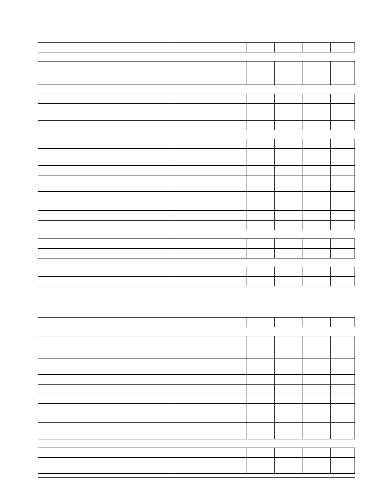
DC ELECTRICAL CHARACTERISTICS (All parameters are specified with Bit 0 of Register 1 set to 1, the rest of the
bits in both registers set to 0, TA = 25°C, VCC = 5.0 V, Iline = 15 mA, f = 1.0 kHz, Test Circuit in Figure 9, unless otherwise noted.)
Parameter
Condition
Min
Typ
Max
Unit
VOLTAGE REGULATION
Line Voltage Vline
Iline = 5.0 mA
Iline = 15 mA
Iline = 60 mA
3.7
4.0
4.3
V
4.2
4.5
4.8
6.6
6.85
7.1
CURRENT REGULATION (Bit 4, Reg.1 = 1; Bit 1, Reg. 2 = 1; RAGC = 47 kΩ)
Line Voltage Vline
Iline = 15 mA
Line Current Iline
Vline = 10 V
Vline = 35 V
4.2
4.5
4.8
V
–
35
–
mA
–
56
–
Line Current Iline in Protection Mode
DC BIASING
Vline = 70 V
–
28
–
mA
Operating Supply Voltage VCC
Current Consumption from VCC
–
3.0
–
5.5
V
VCC = 3.0 V, all Bits to 0
–
3.0
4.0
mA
VCC = 5.0 V, all Bits to 0
–
3.5
4.5
Source Capabiltiy Pin LAO in Speech Mode
Source Capability Pin LAO in Dialing Mode
(Bit 5, Reg. 1 = 1)
VLAO = 0.7 V
VLAO = 0.7 V
–
–
–2.0
mA
–
–
–5.0
mA
Internal Pull Down Resistor at Pin LAO
–
–
11
–
kΩ
Bias Voltage at Pins HYL, HYS and LAI
–
–
1.3
–
V
Bias Voltage at Pins Tx1 and Tx2
Bias Voltage at Pins Rx1 and Rx2
LOGIC INPUTS
Logic Low Level Pins Clk, Data, BEN
–
–
1.5
–
V
–
–
1.3
–
V
–
–
–
0.6
V
Logic High Level Pins Clk, Data, BEN
–
2.2
–
–
V
LOGIC OUTPUTS
Source Capability from Pins HKSW, Out1, Out2
Sink Capability into Pins HKSW, Out1, Out2
Output Voltage at VCC – 1.3 V
–
Output Voltage at 0.5 V
5.0
–
–1.0
mA
–
–
mA
AC ELECTRICAL CHARACTERISTICS (All parameters are specified with Bit 0 of Register 1 set to 1, the rest of the
bits in both registers set to 0, TA = 25°C, VCC = 5.0 V, Iline = 15 mA, f = 1.0 kHz, Test Circuit in Figure 9, unless otherwise noted.)
Parameter
Condition
Min
Typ
Max
Unit
TRANSMIT CHANNEL
Transmit Gain from VTx to Vline
Gain Variation with Line Current Referred to
Iline = 15 mA with the AGC Function Switched “Off”
Gain Increase in 6.0 dB Mode
MC34016P
MC34016DW
VTx = 0.1 Vrms
Iline = 70 mA,
Bit 0, Reg. 2 = 1
Bit 4, Reg. 2 = 1
–1.0
0.25
1.5
dB
–1.25
–0.20
0.85
–0.7
–
0.7
dB
5.3
6.0
6.7
dB
Gain Reduction in Mute Condition
Bit 2, Reg. 2 = 1
65
–
–
dB
Input Impedance at Tx1 or Tx2
–
–
30
Maximum Input Swing for VTx
THD ≤ 2%
–
4.0
THD at the Line (Vline)
VTx = 3.0 dBm
–
1.0
Psophometrically Weighted Noise Level at the Line
200 Ω Between Tx1 and Tx2
–
–79
(Vline)
RECEIVE CHANNEL
Receive Gain from Vline to VRx
Vline = 0.1 Vrms
–1.0
0
Gain Variation with Line Current Referred to
Iline = 15 mA with the AGC Function Switched “Off”
Iline = 70 mA,
Bit 0, Reg. 2 = 1
–0.7
–
–
kΩ
–
Vpp
2.0
%
–
dBmp
1.0
dB
0.7
dB
MOTOROLA ANALOG IC DEVICE DATA
3
Share Link: 