MC74LCX16646DT Ver la hoja de datos (PDF) - Motorola => Freescale
Número de pieza
componentes Descripción
Lista de partido
MC74LCX16646DT Datasheet PDF : 10 Pages
| |||
MOTOROLA
SEMICONDUCTOR TECHNICAL DATA
Advance Information
Low-Voltage CMOS 16-Bit
Transceiver/Registered
Transceiver
With 5V-Tolerant Inputs and Outputs
(3-State, Non-Inverting)
The MC74LCX16646 is a high performance, non–inverting 16–bit
transceiver/registered transceiver operating from a 2.7 to 3.6V supply.
The device is byte controlled. Each byte has separate control inputs
which can be tied together for full 16–bit operation. High impedance TTL
compatible inputs significantly reduce current loading to input drivers
while TTL compatible outputs offer improved switching noise
performance. A VI specification of 5.5V allows MC74LCX16646 inputs to
be safely driven from 5V devices. The MC74LCX16646 is suitable for
memory address driving and all TTL level bus oriented transceiver
applications.
Data on the A or B bus will be clocked into the registers as the
appropriate clock pin goes from a LOW–to–HIGH logic level. Output
Enable (OEn) and Direction Control (DIRn) pins are provided to control
the transceiver outputs. In the transceiver mode, data present at the high
impedance port may be stored in either the A or the B register or in both.
The select controls (SBAn, SABn) can multiplex stored and real–time
(transparent mode) data. The DIR determines which bus will receive data
when OE is active LOW. In the isolation mode (OE HIGH), A data may be
stored in the B register or B data may be stored in the A register. Only one
of the two buses, A or B, may be driven at one time.
MC74LCX16646
LOW–VOLTAGE CMOS
16–BIT TRANSCEIVER/
REGISTERED TRANSCEIVER
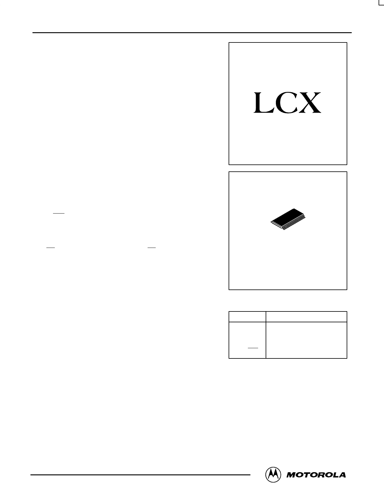
DT SUFFIX
PLASTIC TSSOP PACKAGE
CASE 1202–01
• Designed for 2.7 to 3.6V VCC Operation
• 5.2ns Maximum tpd
• 5V Tolerant — Interface Capability With 5V TTL Logic
• Supports Live Insertion and Withdrawal
• IOFF Specification Guarantees High Impedance When VCC = 0V
• LVTTL Compatible
• LVCMOS Compatible
• 24mA Balanced Output Sink and Source Capability
• Near Zero Static Supply Current in All Three Logic States (20µA)
Substantially Reduces System Power Requirements
• Latchup Performance Exceeds 500mA
• ESD Performance: Human Body Model >2000V; Machine Model >200V
PIN NAMES
Pins
A0–A15
B0–B15
CABn, CBAn
SABn, SBAn
DIRn, OEn
Function
Side A Inputs/Outputs
Side B Inputs/Outputs
Clock Pulse Inputs
Select Control Inputs
Output Enable Inputs
This document contains information on a new product. Specifications and information herein are subject to
change without notice.
11/96
© Motorola, Inc. 1996
1
REV 0.2
Share Link: 