MD59-0039 Ver la hoja de datos (PDF) - Tyco Electronics
Número de pieza
componentes Descripción
Lista de partido
MD59-0039 Datasheet PDF : 7 Pages
| |||
Cellular CDMA Upconverter / Driver, 820 - 850 MHz
MD59-0039
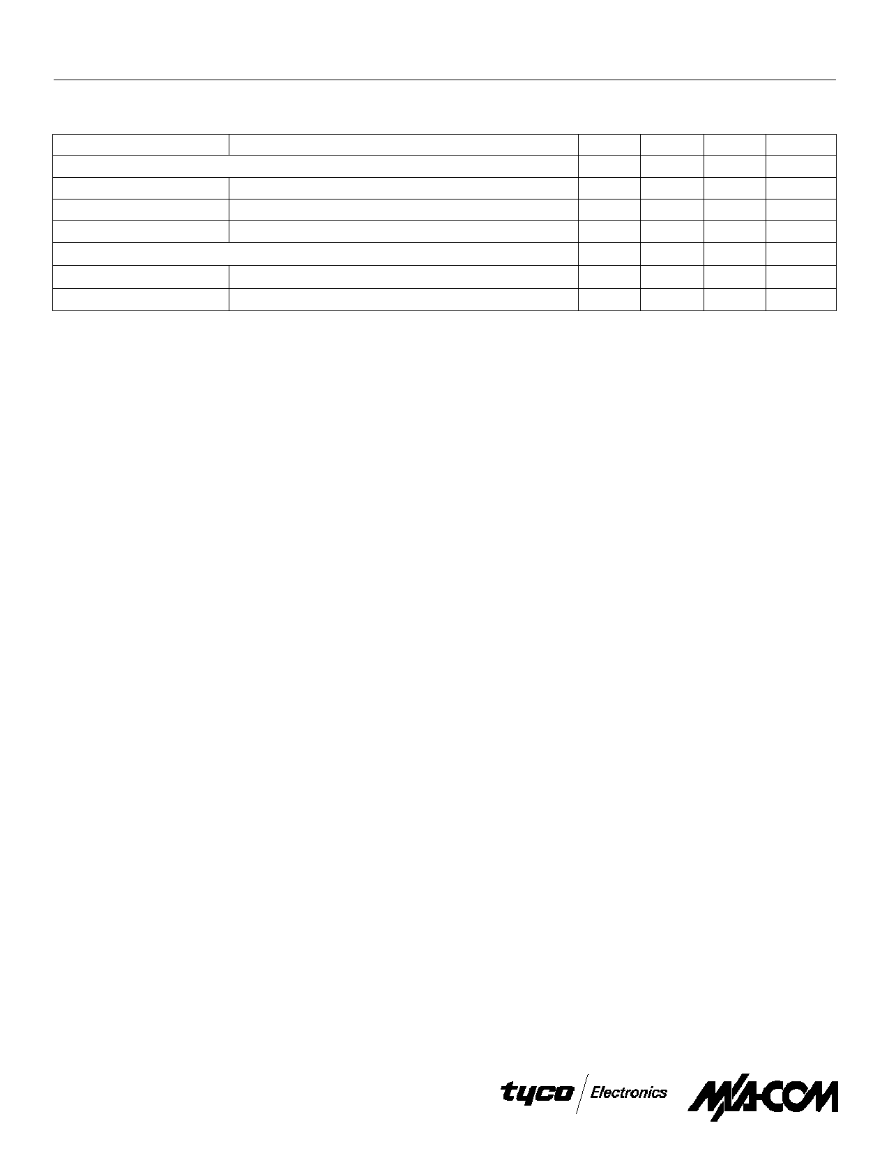
Electrical Specifications TA = +25° C, VDD = 3.0 Volts (Cont’d)
Parameter
Test Conditions
Units
Min.
Typ.
IF Input
IF Frequency
MHz
130
IF Input Level
dBm
IF Impedance
Balanced
ohms
265
LO Input
LO Frequency
MHz
954
LO Input Level
dBm
-10
-5
Max.
-16
979
0
Operating Instructions
The MD59-0039 is a highly integrated MMIC upconverter for
the 800 – 900 MHz cellular band. The upconverter provides
exceptional RF performance while drawing low DC current and
is packaged in a low cost plastic package. It is an ideal
candidate for light-weight, battery operated, portable handset
applications.
The MD59-0039 incorporates a differential IF amplifier,
balanced mixer, LOA, RFA, variable voltage attenuator and a
two-stage driver amplifier. Surface mount resistors, inductors
and capacitors are used in conjunction with the MMIC to
optimize the trade-offs between performance, tunability and
ease of use. The schematic on the previous page shows the
MMIC and required off-chip component values.
The input impedance of the differential IF amplifier is matched
externally to 50 Ω at the desired IF frequency with L1, C1 and
C2. In addition, C1 and C2 also act as DC blocking capacitors
for the differential IF inputs. A 06-03 case style can be used for
L1 in most cases, but a 08-05 case style can be used if more gain
is required. Capacitor C3 is a low frequency bypass capacitor.
Inductors L2 and L3 help match the output of the differential IF
amplifier to the differential input of the mixer, as well as
providing RF chokes for the DC supply lines.
The LO input port is matched on chip to 50 Ω. The LO buffer
amplifier provides the voltage gain required to drive the gate of
the mixer FET, while drawing a minimal amount of current.
The LO buffer amplifies the –10 dBm input signal to the level
required to drive the mixer. For optimum performance, it is
recommended to use a drive level of –3 dBm. C7 and C14 are
RF and low frequency bypass capacitors for the DC supply line.
Capacitor C13 is a source bypass capacitor for the LO amplifier.
The position of both C7 and C13 shown in the application
circuit may affect the gain of the RF amplifier and should be
placed as close the device as is practical.
The mixer is a balanced floating FET mixer that provides
exceptional linearity and isolation with low loss and no DC
current. The mixer uses a high side LO frequency. An external
image reject filter is required between the mixer output and RFA
input to prevent upconversion noise at the image frequency from
leaking onto the RF. This filter should have 50 Ω input and
output impedance.
The topology of both the input and output matching networks
for the RF amplifier provides internal DC blocking capacitors, to
prevent unwanted DC leakage. C6 and C12 are RF and low
frequency bypass capacitors for the DC supply line. Capacitor
C11 is a source bypass capacitor for the RF amplifier. Similar to
the LOA, C11 and C12 should be placed as close the device as is
practical. The VVA is a T-attenuator topology, providing better
than 30 dB of attenuation from 800 to 900 MHz.
The two-stage driver amplifier is nominally biased with 40 mA.
An external resistor, R1, can be used to adjust the bias current of
the second stage, thereby adjusting the linear output power. C4,
C5, C9 and C10 are RF and low frequency bypass capacitors for
the DC supply lines, for the first and second stage of the driver
respectively. Capacitors C8 and C16 are the source bypass
capacitors for the driver amplifier.
Specifications subject to change without notice.
North America: Tel. (800) 366-2266, Fax (800) 618-8883
Asia/Pacific: Tel.+81-44-844-8296, Fax +81-44-844-8298
Europe: Tel. +44 (1344) 869 595, Fax+44 (1344) 300 020
Visit www.macom.com for additional data sheets and product information.
V 2.0
2
Share Link: 