MT90210AL Ver la hoja de datos (PDF) - Mitel Networks
Número de pieza
componentes Descripción
Lista de partido
MT90210AL Datasheet PDF : 27 Pages
| |||
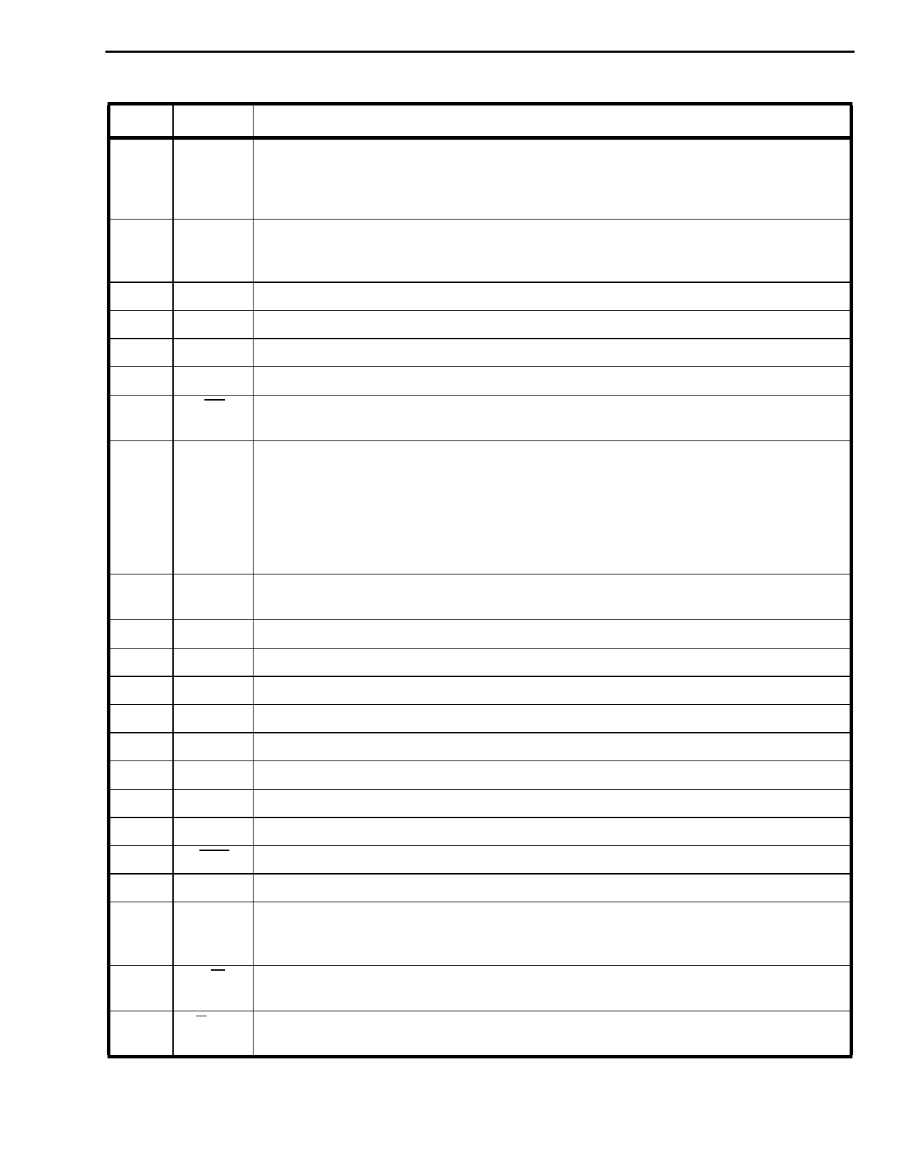
Preliminary Information
MT90210
Pin Description (continued)
Pin
Name
Description
31
SCLK Serial Port Clock (input). The SCLK clock is used to control the serial port operation in
modes 1,2,3 and 4. Depending on the operation mode selected at the MD0-MD2 inputs,
this input can accept 4.096 (MD2-0=000), 8.192 (MD2-0=001) or 16.384 (MD2-0 =010 and
011) MHz clock. In mode 5, this input is ignored.
32
HC4 H-MVIP C4. This is a 4.096 MHz clock utilized in modes 4 and 5 to maintain compatibility
with existing MVIP-90 systems. It is utilized to sample the frame pulse input (F0i). Not used
in Modes 1 - 3.
33
TDI Boundary Scan Test Data Input.
34
TMS Boundary Scan Test Mode Select.
35
TCK Boundary Scan Test Clock.
36
TRST Boundary Scan Test Reset.
37
F0i Frame Synchronization Signal (TTL compatible input). This input signal establishes
the frame boundary for the serial input/output streams.
38-40
MD2-MD0 Operation Mode Bits 0-2 (Input). Selects the data rate for the time division, multiplexed
serial streams. 2.048 (mode 1, MD2-0=000), 4.096 (mode 2, MD2-0=001) or 8.192 (mode
3, MD2-0=010) Mb/s data rates are available. When MD2-0 are set to 011 (mode 4), the
MT90210 operates in mixed data rates mode where S16-23 operate at 8.192 Mb/s and the
remaining serial streams run at 2.048 Mb/s. In mode 5 (MD2-0=100), the MT90210
operates as per mode 4 but the device will accept a differential clock reference at 16.384
MHz at pins C16+ and C16-.
42
C16+ Serial Port Clock Input. In mode 5 (MD2-0= 100), this is a 16.384 MHz differential signal.
Note used in Modes 1 - 3.
43
C16- Serial Port Clock Input. The complement to C16+.
45
TD Reserved - Do not connect.
46
IDDTN Connect to Ground.
47 PLLVSS PLL Ground Input.
48
LP2 Loop Filter Input. An external RC circuit is required at this input, refer to Figure 10.
49
LP1 Loop Filter Input. An external RC circuit is required at this input, refer to Figure 10.
50 PLLAGND PLL Analog Ground output. Provides ground to PLL loop filter, refer to Figure 10.
51 PLLVDD PLL Power Input. +5V
52
RST RESET. A low on this pin resets the device.
53
PCLK Parallel Port Clock Input. CKout must be connected to this input.
54
CKout Internal VCO Output Signal. Output of internal PLL frequency multiplier. In mode 1 the
frequency is 16.384 MHz, for the other modes the frequency is 32.768 MHz. Must be
connected to PCLK only.
56
R/W1 Read/Write Output 1. This output signal toggles low for the last half of a memory write
cycle indicating valid data.
57
R/W2 Read/Write Output 2. This output is low for memory read operations and high for memory
write operations.
2-147
Share Link: 