MGCT03 Ver la hoja de datos (PDF) - Zarlink Semiconductor Inc
Número de pieza
componentes Descripción
Lista de partido
MGCT03 Datasheet PDF : 11 Pages
| |||
MGCT03
IF Variable Gain Amplifier
The filtered IF signal is passed to the IF variable gain
amplifier which in turn drives the single sideband
mixer. An externally applied AGC control voltage
allows the total circuit gain to be varied.
The AGC action is split between the IF and RF
portions of the circuit and an internal AGC control
circuit processes the external AGC control voltage to
drive both IF and RF variable gain amplifiers and
provides a near linear control characteristic over the
entire AGC range.
Single Sideband Mixer
The modulated IF signal is fed to the single sideband
mixer which up-converts the IF to the RF frequency
to be transmitted by mixing with an RF signal from
one of two external UHF oscillator input pins,
seiected by an on chip multiplexer. When 1900MHz
mode is programmed with the VHF oscillator in
divide by four mode (Tables 4 and 5), the polarity of
the quadrature oscillator drive signals to the single
sideband mixer are reversed, thus selecting a low
side LO for 1900MHz PCS and high side for
900MHz. This technique allows a common IF and
filter to be used for both 900MHz and 1900MHz
bands.
RF Variable Gain Amplifier
The SSB mixer is followed by the RF variable gain
amplifier stage which provides about 23dB of the
total gain variation. An additional SAW filter in the
transmit path is avoided by providing the gain
variation after the mixer.
The variable gain amplifier control circuit ensures
that the attenuation from maximum power is initially
controlled by the RF variable gain stage thus
reducing the noise contribution from the RF mixer.
Output Drivers
Separate output drive stages are provided for
900MHz and 1900MHz operation. A differential
design is used for both amplifiers to improve power
efficiency and to ease power supply decoupling
problems. The 900MHz output stage provides a
linear output of 8dBm for TDMA operation, but is
over-driven in AMPS mode to obtain a typical output
of 11dBm. In both power driver stages the DC
current is backed off as the RF and IF gain is
reduced, improving efficiency when less than
maximum output power is required.
Control Inputs
Three control inputs are provided to select different
operating modes for the chip; the various modes
selected by the control pins are shown in Tables 4
and 5.
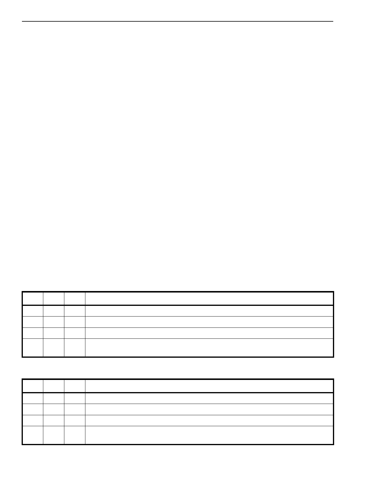
CP2 CP1 CP0
Function
0
0
0 Sleep mode. All circuits powered down
0
0
1 Quadrature modulator on. 1900MHz mode. Low side UHF LO. IF = VHF VCO ÷ 4
0
1
0 Quadrature modulator on. 900MHz mode. high side UHF LO. IF = VHF VCO ÷ 4
0
1
1 Standby mode. VHF oscillator input buffer, oscillator bias on. All other circuits powered
down
Table 4 - Control pin functions; VHF LO in divide-by-four mode
CP2 CP1 CP0
Function
1
0
0 Sleep mode. All circuits powered down
1
0
1 Quadrature modulator on. 1900MHz mode. Low side UHF LO. IF = VHF VCO ÷ 2
1
1
0 Quadrature modulator on. 900MHz mode. high side UHF LO. IF = VHF VCO ÷ 2
1
1
1 Standby mode. VHF oscillator input buffer, oscillator bias on. All other circuits powered
down
Table 5 - Control pin functions; VHF LO in divide-by-two mode
6
Share Link: 