FSTU6800(1999) Ver la hoja de datos (PDF) - Fairchild Semiconductor
Número de pieza
componentes Descripción
Lista de partido
FSTU6800
(Rev.:1999)
(Rev.:1999)
Fairchild Semiconductor

FSTU6800 Datasheet PDF : 5 Pages
| |||
AC Electrical Characteristics
Symbol
Parameter
TA = −40 °C to +85 °C,
CL = 50 pF, RU = RD = 500Ω
VCC = 4.5 – 5.5V
VCC = 4.0V
Units
Conditions
Figure No.
Min
Max
Min
Max
tPHL,tPLH Prop Delay Bus to Bus (Note 6)
0.25
0.25
ns
VI = OPEN
Figure 1
Figure 2
tPZH
Output Enable Time
tPZL
7.0
30.0
7.0
30.0
35.0
ns
VI = OPEN
BiasV = GND
35.0
ns
VI = 7V
BiasV = 3V
Figure 1
Figure 2
tPHZ
Output Disable Time
tPLZ
1.0
6.1
1.0
7.3
6.5
ns
VI = OPEN
BiasV = GND
6.8
ns
VI = 7V
BiasV = 3V
Figure 1
Figure 2
Note 6: This parameter is guaranteed by design but is not tested. The bus switch contributes no propagation delay other than the RC delay of the typical On
resistance of the switch and the 50 pF load capacitance, when driven by an ideal voltage the source (zero output impedance).
Capacitance (Note 7)
Symbol
Parameter
Typ
Max
Units
Conditions
CIN
Control Pin Input Capacitance
3
CI/O
Input/Output Capacitance
5
Note 7: TA = +25°C, f = 1 MHz, Capacitance is characterized but not tested.
pF
VCC = 5.0V
pF
VCC, OE = 5.0V
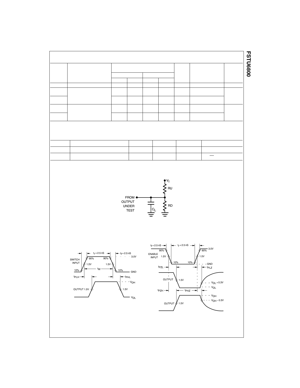
AC Loading and Waveforms
Note: Input driven by 50 Ω source terminated in 50 Ω, RU = RD = 500 Ω
Note: CL includes load and stray capacitance, CL= 50 pF
Note: Input PRR = 1.0 MHz, tW = 500 nS
FIGURE 1. AC Test Circuit
FIGURE 2. AC Waveforms
3
www.fairchildsemi.com
Share Link: