MRFIC1884 Ver la hoja de datos (PDF) - Motorola => Freescale
Número de pieza
componentes Descripción
Lista de partido
MRFIC1884 Datasheet PDF : 4 Pages
| |||
MRFIC1884
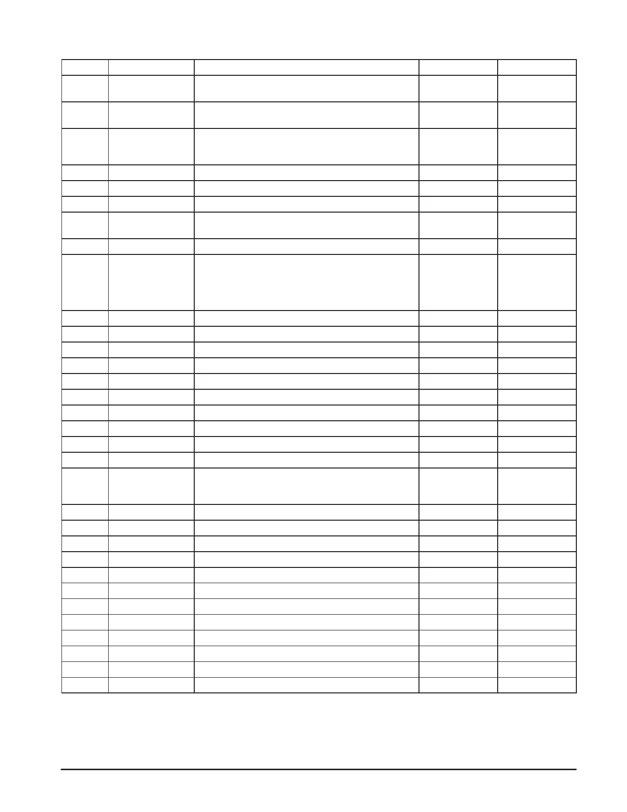
PIN FUNCTION DESCRIPTION
Pin
Function
Description
Voltage On (V)
Voltage Off (V)
1
Band
Band Selection pin. A logic ”High” (>2.4 V) selects PCS
2.4 to 3.2
0 to 0.4
band and ”Low” (<0.4 V) selects Cellular band.
2
Mode
Mode selection pin. A logic ”High” (>2.4 V) selects CDMA
2.4 to 3.2
0 to 0.4
band and ”Low” (<0.4 V) selects AMPS band.
3
Exciter Out
Cellular band RF Exciter output pin.
(Cellular)/
VCC1
4
Gnd
Ground connection.
2.7 to 3.2
–
5
VCC2
Supply Voltage.
6
Gnd
Ground connection.
2.7 to 3.2
–
7
Exciter Out (PCS)/ PCS band RF Exciter output pin.
VCC3
8
Gnd
Ground connection.
2.7 to 3.2
–
9
Tx Enable
Tx Enable pin. A logic ”High” (>2.4 V) enables Tx path and
2.4 to 3.2
”Low” (<0.4 V) diables Tx path except LO Buffer and
bandgap reference (will disable the entire chip complete
with Band selection pin and Mode selection pin, refer to
Table ?).
0 to 0.4
10
VCC4
Supply Voltage.
11
Gnd
Ground connection.
2.7 to 3.2
–
12
Exciter In (PCS)
PCS band RF Exciter input pin.
–
13
Gnd
Ground connection.
–
14
Mixer Out– (PCS) PCS band Mixer RF output pin.
2.7 to 3.2
15
Mixer Out+ (PCS) PCS band Mixer RF output pin.
2.7 to 3.2
16
VCC5
Supply Voltage.
17
Gnd
Ground connection.
2.7 to 3.2
–
18
LO (PCS)
PCS band Mixer LO input pin.
–12 dBm (Typ)
19
Gnd
Ground connection.
–
20
Vgc
RF AGC control pin. A 30 dB dynamic range can be
0.1 to 1.7
achieved by adjusting voltage from 0.1 V (low gain) to 1.7
V (high gain).
21
IF In–
Mixer IF input pin.
–23 dBm (Typ)
22
IF In+
Mixer IF input pin.
–23 dBm (Typ)
23
VCC6
Supply Voltage.
24
LO (Cellular)
Cellular band Mixer LO input pin.
2.7 to 3.2
–13 dBm (Typ)
25
Gnd
Ground connection.
–
26
VCC7
Supply Voltage.
27
Mixer Out+ (Cellular) Cellular band Mixer RF output pin.
2.7 to 3.2
2.7 to 3.2
28
Mixer Out– (Cellular) Cellular band Mixer RF output pin.
2.7 to 3.2
29
Gnd
Ground connection.
–
30
Exciter In (Cellular) Cellular band RF Exciter input pin.
–
31
Gnd
Ground connection.
–
32
VCC8
Supply Voltage.
2.7 to 3.2
2
MOTOROLA WIRELESS SEMICONDUCTOR
SOLUTIONS – RF AND IF DEVICE DATA
Share Link: 