MSM6948 Ver la hoja de datos (PDF) - Oki Electric Industry
Número de pieza
componentes Descripción
Lista de partido
MSM6948 Datasheet PDF : 13 Pages
| |||
¡ Semiconductor
MSM6948/6948V
PIN DESCRIPTION
Name
X1
X2
*MCK
ME
Description
Crystal connection pins.
A 3.6864 MHz crystal shall be connected.
When an external clock is applied for MSM6948's oscillation source, it has to be input to X2.
In this case, X2 has to be AC-coupled by the capacitor of 200 pF. X1 shall be left open.
3.6864 MHz ±0.02% clock output.
This can be used for other devices under limited load conditions.
When digital "1" is put on this pin, MSK modulator output is connected to the input of
transmit LPF.
When digital "0" is put on, the input of transmit LPF is connected to TI that is voice signal input.
The data put on ME terminal is synchronized with the rising edge of ST and input to internal
logic as a control data. The rising edge of this synchronized data resets MSK modulator.
Transmit data input.
The data on this pin is synchronized with the rising edge of ST and input to MSK modulator
as an actual transmit data.
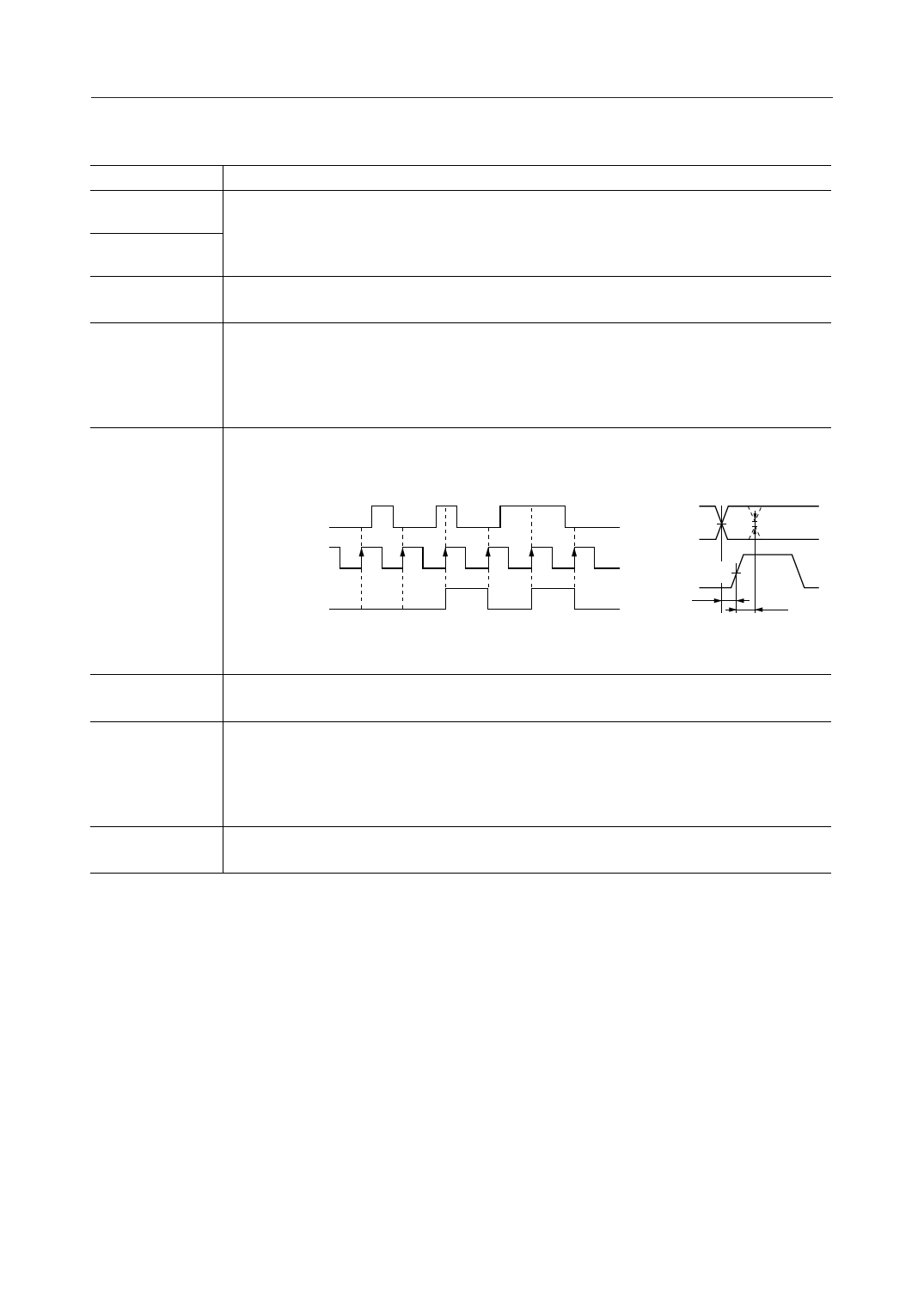
SD
SD
ST
MSK
Modulated
Data
SD 50%
SD 50%
tsetup
thold
tsetup; Min. 300 ns
thold ; Min. 300 ns
ST
ST is synchronizing signal used for ME and SD.
This is made from master clock and is usually 1200 Hz.
Built-in analog signal ground.
The DC voltage is approximately half of VDD, so the analog signals of AI, AO, and TI interfaces
SG
with peripheral circuits which must be implemented by AC-coupling. To make this voltage
source impedance lower and ensure the device performance, it is necessary to put a bypass
capacitor on SG in close physical proximity to the device.
AG
Analog ground.
This pin should be common with DG at the system ground point as close as possible.
*NC : MSM6948V
4/13
Share Link: 