MSM7532 Ver la hoja de datos (PDF) - Oki Electric Industry
Número de pieza
componentes Descripción
Lista de partido
MSM7532 Datasheet PDF : 21 Pages
| |||
¡ Semiconductor
MSM7532
SD
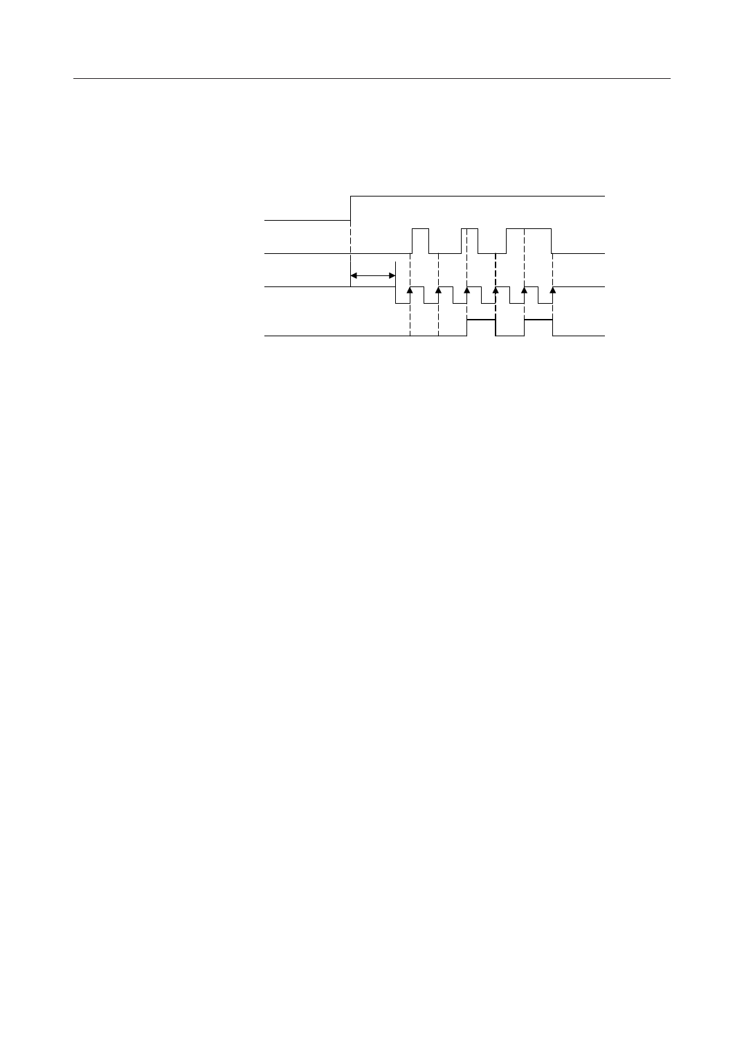
Transmit data input pin.
The data on the SD pin is accepted as the modulator input signals in synchronization with the rising
edges of ST.
ME
SD Input
tMS
ST
Modulator Input Data
At the start of data transmission, the synchronization with the receive modem is required. Therefore
bit synchronous signals (the alternating patterns of "1" and "0") more than 18 bits should be input in
SD.
If a radio transmission path is better in S/N ratio, the receive section can properly operate with bit
synchronous signals more than 11 bits.
FD
Frame synchronous detection signal output pin.
If the contents of received data in the LSI matches the patterns defined by FPS and BIT in a state
where FDE is at "1" level, FD holds "1" level. If FDE is at"0" level, FD is fixed at "0" level. FD is also
fixed at "0" in power-down mode 1 or 2 (PDN = "1", RVE = "0").
Take the following procedure to detect frame synchronization:
(1) Set the synchronous patterns to be detected at BIT and FPS.
(2) Drive FDE at "0" level for 1 ms or more, and then at "1" level. FD is reset to "0" and RT and PD are
fixed at "1" level.
(3) When a frame synchronous signal has been detected, FD is driven at "1" level and RT and RD
become active. To ensure detection of frame synchronous signals, lock in PLL of the receive modem.
At the beginning of transmission, transmit synchronous patterns after synchronizing with the
opposite modem using a bit synchronous signal of 18 bits or more.
Refor to "Receiver Signal Timing" in Fig. 3.
RD
Receive data output pin.
Outputs demodulation serial data for receive signals.
Since the RD data is output in synchronization with the falling edges of re-generated timing clock
pulse RT, it is recommended that the data be latched on the rising edge of RT.
If FDE is at "1" level and FD is at "0" level, RD remains set at "1" level.
11/21
Share Link: 