MSM7566 Ver la hoja de datos (PDF) - Oki Electric Industry
Número de pieza
componentes Descripción
Lista de partido
MSM7566 Datasheet PDF : 19 Pages
| |||
¡ Semiconductor
MSM7566/7567
VFRO
Receive filter output.
The output signal has an amplitude of 2.4 VPP above and below the signal ground voltage (SG)
when the digital signal of +3 dBmO is input to PCMIN and can drive a load of 20 kW or more.
For driving a load of 20 kW or less, connect a resistor of 20 kW or more should be connected
between the pins VFRO and PWI.
When adding the frequency characteristics to the receive signal, refer to the application example.
During power saving mode, the output of VFRO is at the voltage level of SG. During power down
mode, the output is in a high impedance state.
PWI, AOUT+, AOUT–
PWI is connected to the inverting input of the receive driver. The receive driver output is
connected to the AOUT– pin. Therefore, the receive level can be adjusted with the pins VFRO,
PWI, and AOUT–. When the PWI pin is not used, the PWI pin to the AOUT– pin, and leave open
the pins AOUT– and AOUT+. The output of AOUT+ is inverted with respect to the output of
AOUT–. Since the signal from which provides differential drive of an impedance of 1.2 kW +55
nF, these outputs can directly be connected to a receiver of handset using a piezoelectric
earphone.
Refer to the application example.
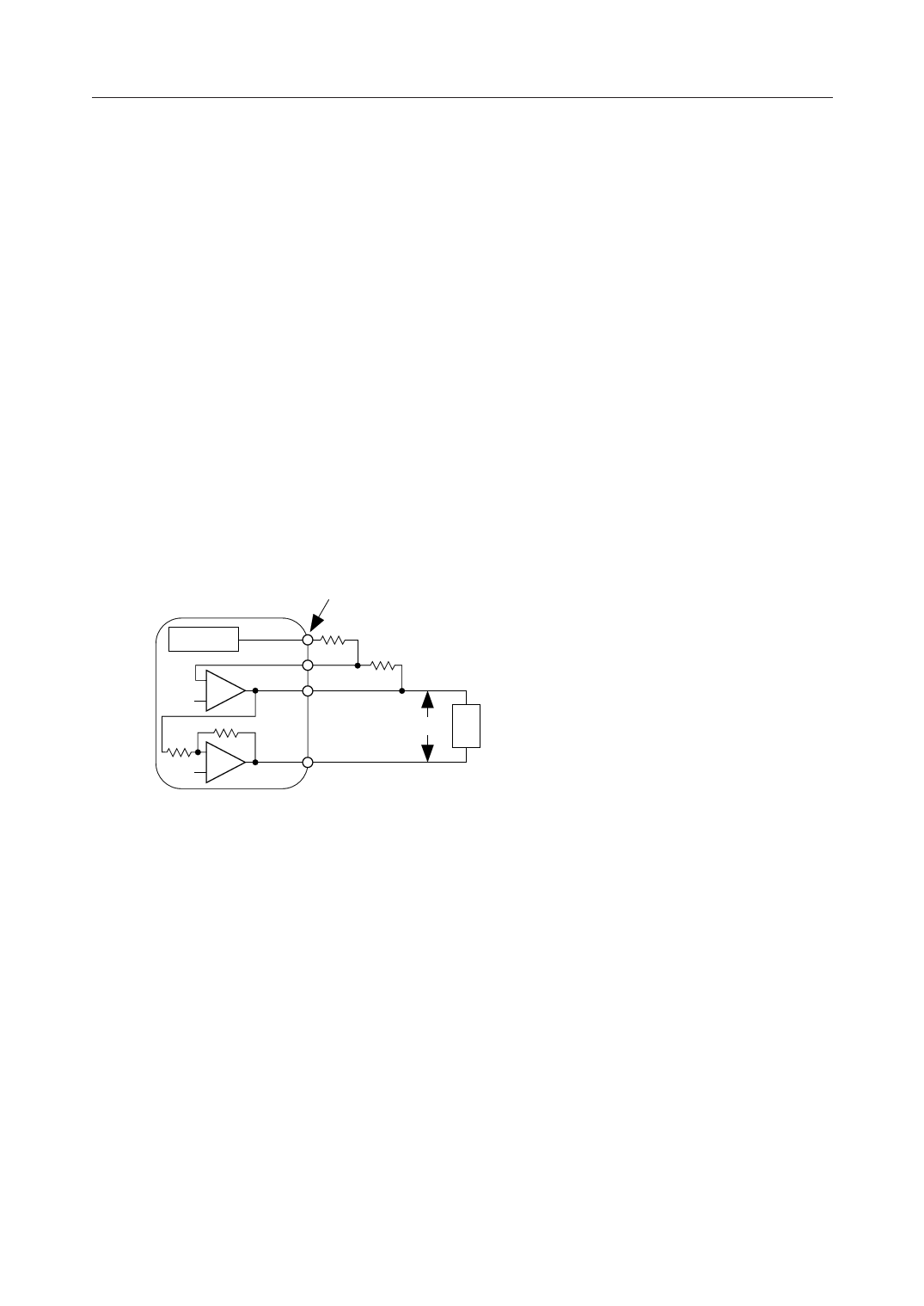
VI
Receive Filter
VFRO R6
PWI
R7
–
SG +
AOUT–
VO ZL
–
SG +
AOUT+
R6 > 20 kW
ZL ≥ 2.4 kW
Gain = VO/VI = 2 ¥ R7/R6 £ 2
The other external signals can be output from AOUT+ and AOUT– during power saving, since
these driver amplifiers are in the operational state. During power down mode, the output of
AOUT+ and AOUT– is at the voltage level of SG through high impedance.
The electrical driving capability of the AOUT– pin and AOUT+ pin is ±1.3 V maximum. The
output load resistor has a minimum value of 1.2 kW.
If an output amplitude less than ±1.3 V is allowed, these outputs can drive a load resistance less
than that described above. For more details, refer to SINGLE POWER SUPPLY PCM CODEC
APPLICATION NOTE.
VDD
Power supply for +2.7 V to +3.8 V. (Typically 3.0 V)
PCMIN
PCM signal input.
A serial PCM signal input to this pin is converted to an analog signal in synchronization with the
RSYNC signal and BCLOCK signal.
The data rate of the PCM signal is equal to the frequency of the BCLOCK signal.
The PCM signal is shifted at a falling edge of the BCLOCK signal and latched into the internal
register when shifted by eight bits.
The start of the PCM data (MSD) is identified at the rising edge of RSYNC.
5/19
Share Link: 