MSM7582TS-K Ver la hoja de datos (PDF) - Oki Electric Industry
Número de pieza
componentes Descripción
Lista de partido
MSM7582TS-K Datasheet PDF : 24 Pages
| |||
¡ Semiconductor
MSM7582/7582B
SLS2, SLS1
Receiver slot select signal inputs.
The devices have four sets of clock recovery circuit to each channel and four AFC information
storage registers. One these circuits is selected from a combination of the signals at these pins.
(SLS2, SLS1) = (0, 0): Slot 1, (0, 1): Slot 2
(1, 0): Slot 3, (1, 1): Slot 4
RPR
High-speed phase clock control signal input for the clock recovery circuit.
If this pin is “1”, the clock recovery circuit starts in the high-speed phase clock mode. When the
phase difference is less than a defined value, the circuit shifts to the low-speed phase clock mode
automatically. When this pin is “0”, the circuit is always in the low-speed phase clock mode.
AFC
AFC operation range specification signal input.
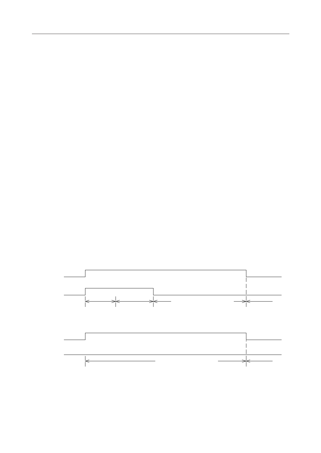
As shown in Fig. 4, the AFC information is reset when both AFC and RPR are set to “1”. AFC
operation starts after a fixed number of clock cycles and after the AFC information is reset. If RPR
is set to “1”, an average number of times that AFC turns on is low. If RPR is “0”, AFC is high. If
AFC is “0”, frequency error is not calculated, but the frequency is corrected using an error that
is held.
RCW
Clock recovery circuit operation ON/OFF control signal input. If RCW pin is “0”, DPLL does not
make any phase corrections.
(CASE1)
AFC
RPR
(CASE2)
AFC
RPR
AFC information
is reset.
Average
number of times
AFC is low.
Average number of times
AFC is high.
The clock recovery circuit
starts with the previous
AFC information.
"0"
Average number of times
AFC is high.
Figure 4 AFC Control Timing Diagram
AFC information
is maintained.
AFC information
is maintained.
9/24
Share Link: 