MT9126AS Ver la hoja de datos (PDF) - Mitel Networks
Número de pieza
componentes Descripción
Lista de partido
MT9126AS Datasheet PDF : 22 Pages
| |||
MT9126
Preliminary Information
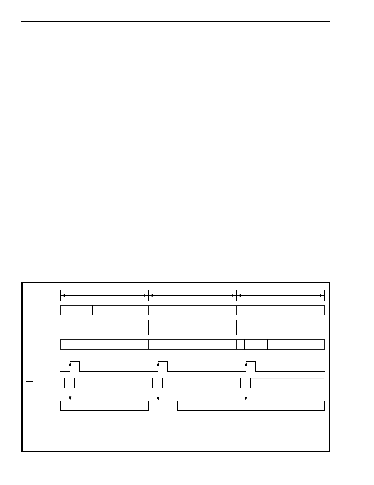
Processing Delay Through the Device
Applications
In order to accommodate variable rate PCM and
ADPCM interfaces, the serial input and output
streams require a complete frame to load internal
shift registers. Internal frame alignment of the
encoding/decoding functions are taken from either of
the F0i or ENB1 & ENB2 input strobes depending
upon the device operating mode (i.e., ST-BUS or
SSI). The encoding/decoding of all channels then
takes one frame to complete before the output
buffers are loaded. This results in a two frame
transcoding delay. The two frame delay also applies
to the D and C channels and to the PCM and
ADPCM bypass functions.(See Figure 10.)
Note: When changing the relative positions of the
ENB1 and ENB2 strobes, precaution must be taken
to ensure that two conditions are met. They are:
1) There must be at least 512 master clock cycles
between consecutive rising edges of ENB1. This
condition also holds true for ENB2.
2) The ENB1 strobe must alternate with the ENB2
strobe.
Violation of these requirements may cause noise on
the output channels.
Figure 11 depicts an ISDN line card utilizing the
MT8910 ’U’ interface transciever and MT9126
ADPCM transcoder. This central office application
implements the network end of a Pair-Gain system.
Figure 12 shows Mitel devices used to construct the
remote Pair-Gain loop terminator.
Figure 13 depicts an ADPCM to linear PCM
converter for applications where further, value
added, functions are being performed via digital
signal processor. Access to linear coded PCM
reduces the overhead of the DSP by removing the
need for a companded to linear conversion. The
linear PCM capability of the ADPCM transcoder in
conjunction with the frame alignment signal EN1
allows direct connection to the serial port of both
Motorola and Texas Instruments Digital Signal
Processors. Daisy-chaining via the delayed frame
strobe output ensures that the ADPCM array is
distributed over the complete 2048 kbit bandwidth. If
the DSP has a second serial port then access to the
processed PCM can be had directly. For processors
with only one serial port the MT8920 connected to
the DSP parallel port will provide serial access by
parallel to serial conversion. The same daisy-
chained arrangement of Quad ADPCM transcoders
will provide a general system resource for PCM-
ADPCM conversion by setting the device to non-
linear operation.
PCMi1/2
ADPCMo
frame n-1
frame n
Byte "x"
PCM Byte "X" latched into device
during frame n-1
PCM Byte "X" processed according
to MSn input states latched during
frame n
frame n+1
ADPCM Word "X" output from
device during frame n+1
Word "x"
ENB1 or ENB2
F0i
MS1 or 4
AAAAAAAAAAAAAAAAA
32 kb/s
AAAAAAAAAAAAAAAAAAAAAAAAAAAA
24 kb/s
AAAAAAAAAAAAAAAAAAAAAAAAAAAA
32 kb/s
Where MS2, 3, 5, 6 = 0
This diagram shows the conversion sequence from PCM to ADPCM. The same pipelining occurs in the
reverse ADPCM to PCM direction.
Total delay from data input to data output = 2 frames.
Figure 10 - Data Throughput
8-46
Share Link: 