MT9126AS Ver la hoja de datos (PDF) - Mitel Networks
Número de pieza
componentes Descripción
Lista de partido
MT9126AS Datasheet PDF : 22 Pages
| |||
MT9126
Preliminary Information
EN1 1
MCLK 2
F0i 3
C2o 4
BCLK 5
PCMo1 6
PCMi1 7
VSS 8
LINEAR 9
ENB2/F0od 10
ENB1 11
PCMo2 12
PCMi2 13
SEL 14
28 EN2
27 MS6
26 MS5
25 MS4
24 ADPCMo
23 ADPCMi
22 VDD
21 MS3
20 MS2
19 MS1
18 IC
17 PWRDN
16 FORMAT
15 A/µ
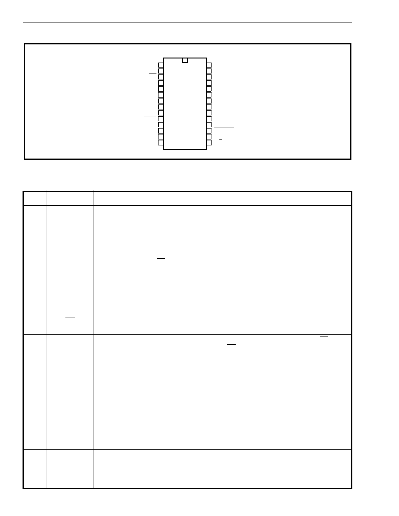
Figure 2 - Pin Connections
Pin Description
Pin #
1
2
Name
EN1
MCLK
Description
Enable Strobe 1 (Output). This 8 bit wide, active high strobe is active during the B1
PCM channel in ST-BUS mode. Becomes a single bit, high true pulse when LINEAR=1.
In SSI mode this output is high impedance.
Master Clock (input). This is a 4.096 MHz (minimum) input clock utilized by the
transcoder function; it must be supplied in both ST-BUS and SSI modes of operation.
In ST-BUS mode the C4 ST-BUS clock is applied to this pin. This synchronous clock is
also used to control the data I/O flow on the PCM and ADPCM input/output pins
according to ST-BUS requirements.
In SSI mode this master clock input is derived from an external source and may be
asynchronous with respect to the 8 kHz frame. MCLK rates greater than 4.096 MHz are
acceptable in this mode since the data I/O rate is governed by BCLK.
3
F0i
Frame Pulse (Input). Frame synchronization pulse input for ST-BUS operation. SSI
operation is enabled by connecting this pin to VSS.
4
C2o
2.048 MHz Clock (Output). This ST-BUS mode bit clock output is the MCLK (C4) input
divided by two, inverted, and synchronized to F0i. This output is high-impedance during
SSI operation.
5
BCLK Bit Clock (Input). 128 kHz to 4096 kHz bit clock input for both PCM and ADPCM ports;
used in SSI mode only. The falling edge of this clock latches data into ADPCMi, PCMi1
and PCMi2. The rising edge clocks data out on ADPCMo, PCMo1 and PCMo2. This input
must be tied to VSS for ST-BUS operation.
6
PCMo1 Serial PCM Stream 1 (Output). 128 kbit/s to 4096 kbit/s serial companded/linear PCM
output stream. Data are clocked out by rising edge of BCLK in SSI mode. Clocked out by
MCLK divided by two in ST-BUS mode. See Figure 14.
7
PCMi1 Serial PCM Stream 1 (Input). 128 kbit/s to 4096 kbit/s serial companded/linear PCM
input stream. Data are clocked in on falling edge of BCLK in SSI mode. Clocked in at the
3/4 bit position of MCLK in ST-BUS mode. See Figure 14.
8
VSS
Digital Ground. Nominally 0 volts.
9
LINEAR Linear PCM Select (Input). When tied to VDD the PCM I/O ports (PCM1,PCM2) are 16-
bit linear PCM. Linear PCM operates only at a bit rate of 2048 kbit/s. Companded PCM is
selected when this pin is tied to VSS. See Figures 5 & 8.
8-34
Share Link: 