CY7C4231-25JC Ver la hoja de datos (PDF) - Cypress Semiconductor
Número de pieza
componentes Descripción
Lista de partido
CY7C4231-25JC Datasheet PDF : 21 Pages
| |||
CY7C4421/4201/4211/4221
CY7C4231/4241/4251
Switching Waveforms (continued)
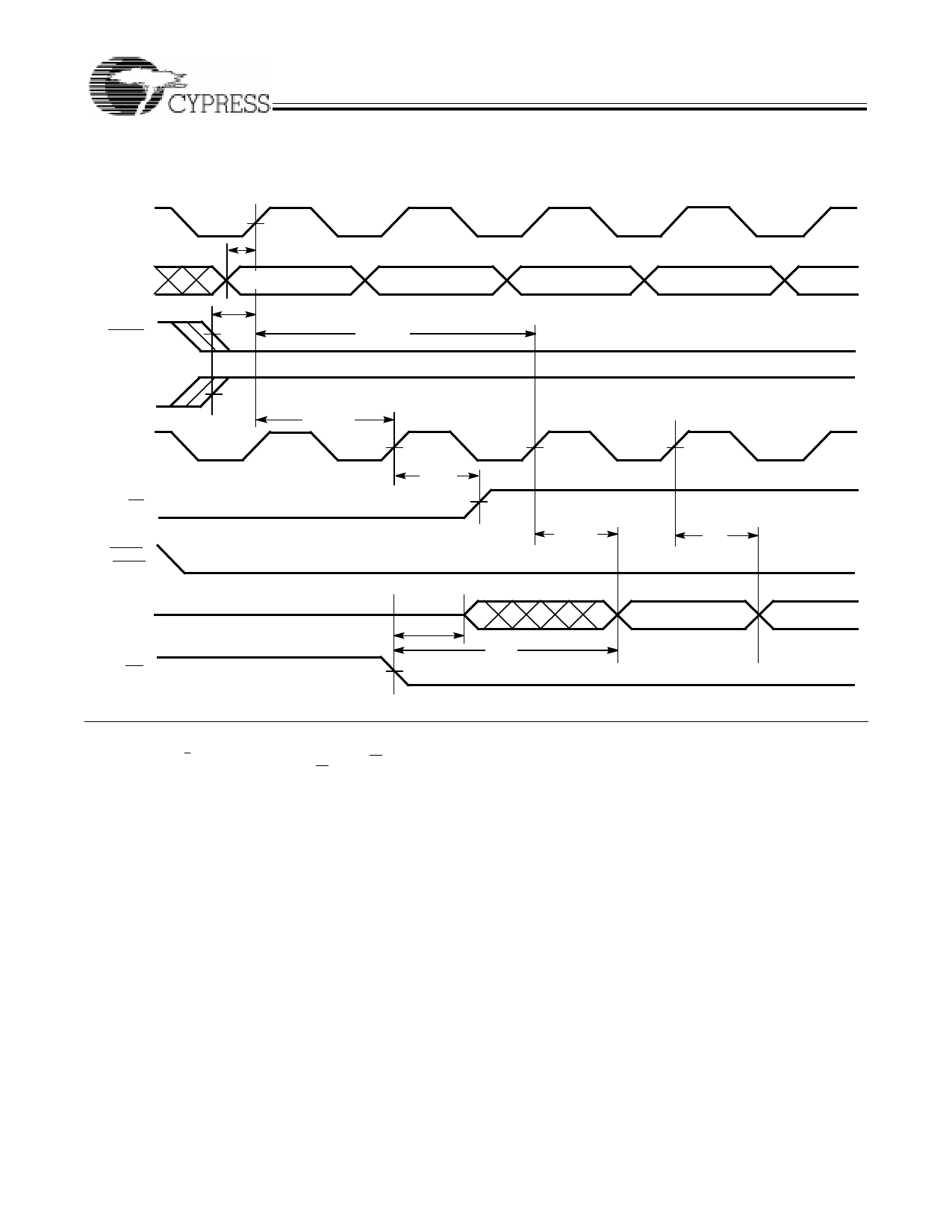
First Data Word Latency after Reset with Simultaneous Read and Write
WCLK
tDS
D0 –D8
D0 (FIRSTVALID WRITE)
D1
D2
WEN1
tENS
[16]
tFRL
WEN2
(if applicable)
RCLK
EF
REN1,
REN2
tSKEW1
tREF
tA [17]
D3
D4
tA
Q0 –Q8
OE
tOLZ
tOE
D0
D1
42X1–9
Notes:
16. When tSKEW1 > minimum specification, tFRL (maximum) = tCLK + tSKEW1. When tSKEW1 < minimum specification, tFRL (maximum) = either 2*tCLK + tSKEW1 or tCLK + tSKEW1.
The Latency Timing applies only at the Empty Boundary (EF = LOW).
17. The first word is available the cycle after EF goes HIGH, always.
8
Share Link: 