NB2309AC1HDG Ver la hoja de datos (PDF) - ON Semiconductor
Número de pieza
componentes Descripción
Lista de partido
NB2309AC1HDG Datasheet PDF : 9 Pages
| |||
NB2309A
Zero Delay and Skew Control
All outputs should be uniformly loaded to achieve Zero
Delay between input and output. Since the CLKOUT pin is
the internal feedback to the PLL, its relative loading can
adjust the input−output delay.
For applications requiring zero input−output delay, all
outputs, including CLKOUT, must be equally loaded. Even
if CLKOUT is not used, it must have a capacitive load equal
to that on other outputs, for obtaining zero−input−output
delay.
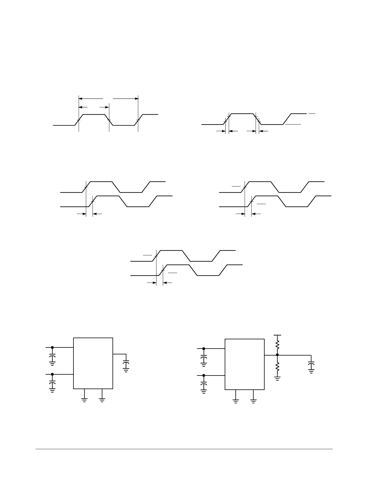
SWITCHING WAVEFORMS
1.4 V
t1
t2
1.4 V
1.4 V
Figure 3. Duty Cycle Timing
OUTPUT
2.0 V
0.8 V
t3
2.0 V
0.8 V
t4
3.3 V
0V
Figure 4. All Outputs Rise/Fall Time
OUTPUT
OUTPUT
1.4 V
t5
1.4 V
Figure 5. Output − Output Skew
VDD
2
INPUT
VDD
OUTPUT
2
t6
Figure 6. Input − Output Propagation Delay
CLKOUT, Device 1
CLKOUT, Device 2
VDD
2
t7
VDD
2
Figure 7. Device − Device Skew
VDD
CLKOUT
0.1 mF
OUTPUTS
CLOAD
VDD
0.1 mF GND GND
TEST CIRCUITS
VDD
0.1 mF
OUTPUTS
VDD
0.1 mF GND GND
VDD
1 kW
1 kW
10 pF
Figure 8. Test Circuit #1
Figure 9. Test Circuit #2
For parameter t8 (output slew rate) on −1H devices
http://onsemi.com
6
Share Link: 