NCP1000P Ver la hoja de datos (PDF) - ON Semiconductor
Número de pieza
componentes Descripción
Lista de partido
NCP1000P Datasheet PDF : 14 Pages
| |||
NCP1000, NCP1001, NCP1002
Applications
Do not attempt to construct a converter circuit on a
wire−wrap or plug−in prototype board. In order to ensure
proper device operation and stability, it is important to
minimize the lead length and the associated inductance of
the ground pin. This pin must connect as directly as possible
to the printed circuit ground plane and should not be bent or
offset by the board layout. The Power Switch Circuit pin can
be offset if additional layout creepage distance is required.
Due to the potentially high rate of change in switch current,
a capacitor (if used), at pin 2, should have traces as short as
possible, from pin 2 and ground. This will significantly
reduce the level of switching noise that can be imposed upon
the feedback control signal.
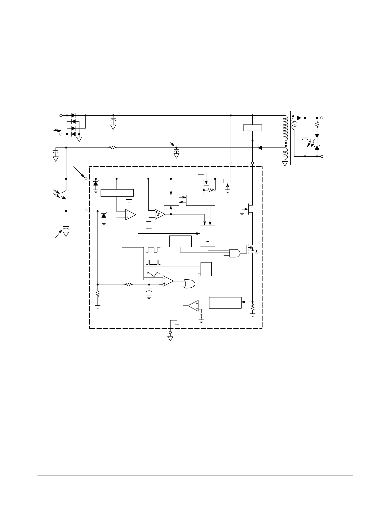
AC Line
+
Input
Snubber
Bypass
+
Auto Restart Timing
VCC
Auxiliary Output
+
Startup
4
1
Feedback
Input
2
+
Loop Compensation
10 V
VCC Limiter 8.6 V
10 V
Opto Fail−safe
Startup
Internal
Bias
State Control
Power up−reset
10 mA
Oscillator
Duty Cycle
Clock
Ramp
+ Undervoltage
8.5 V/ Lockout
7.5 V
Thermal
Shutdown
Ck R
Divide
by 8
Q
PWM Latch
S
Q
R
Driver
Power Switch
Circuit
5
7.0 kHz
Filter
2.7 k
PWM
Comparator
Current Limit
Comparator
Leading Edge
Blanking
+
Rpk
Ground 3
Figure 17. Representative Block Diagram
+
+
Converter
DC Output
−
http://onsemi.com
11
Share Link: 