NCP1027 Ver la hoja de datos (PDF) - ON Semiconductor
Número de pieza
componentes Descripción
Lista de partido
NCP1027
ON Semiconductor

NCP1027 Datasheet PDF : 30 Pages
| |||
NCP1027
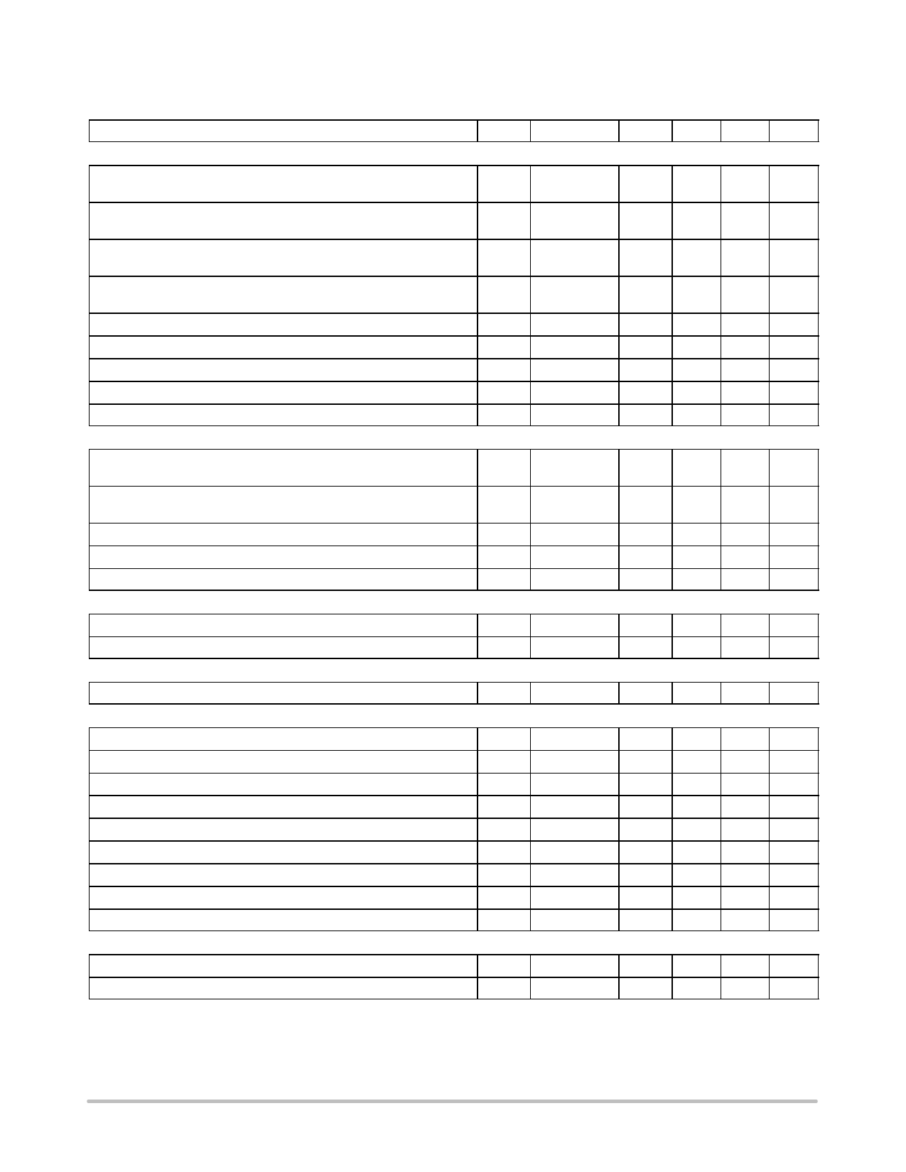
ELECTRICAL CHARACTERISTICS (continued) (For typical values TJ = 25°C, for min/max values TJ = 0°C to +125°C,
Max TJ = 150°C, VCC = 8.0 V, unless otherwise noted.)
Characteristic
Pin
Symbol
Min
Typ Max Unit
CURRENT COMPARATOR
Maximum Internal Current Setpoint, Pin 4 Open, TJ = 25°C,
FSW = 65 kHz (Note 3)
Final Switch Current with a Primary Slope of 200 mA/ms,
FSW = 65 kHz (Note 4)
−
Ipeak_27_CS_ 720
800
880
mA
65 k
− Ipeak_27_SW_ −
820
−
mA
65 k
Maximum Internal Current Setpoint, Pin 4 Open, TJ = 25°C,
FSW = 100 kHz (Note 3)
Final Switch Current with a Primary Slope of 200 mA/ms,
FSW = 100 kHz (Note 4)
Setpoint Decrease for a Pin 7 Injected Current of 40 mA, TJ = 25°C
Voltage Level in Pin 7 at which OPP Starts to Operate
−
Ipeak_27_CS_ 720
800
880
mA
100 k
− Ipeak_27_SW_ −
820
−
mA
100 k
7
IOPP
−
23
−
%
7
IOPPtripV
−
1.5
−
V
Soft−Start Duration
Propagation Delay from Current Detection to Drain OFF State
Leading Edge Blanking Duration
INTERNAL OSCILLATOR
−
TSS
−
1.0
−
ms
−
Tprop
−
100
−
ns
−
TLEB
−
200
−
ns
Oscillation Frequency (Note 5)
65 kHz Version, TJ = 25°C
−
fOSC
kHz
58.5
65 71.5
Oscillation Frequency (Note 5)
100 kHz Version, TJ = 25°C
−
fOSC
kHz
90
100 110
Frequency Jittering in Percentage of fOSC
Jittering Swing Frequency
−
fJitter
−
"6.0
−
%
−
fswing
−
300
−
Hz
Maximum Duty Cycle
−
Dmax
74
80
87
%
FEEDBACK SECTION
Internal Pullup Resistor
4
Rupp
−
16
−
kW
Ramp Compensation Level on Pin 1 – Rramp = 100 kW
2
Rlevel
−
2.75
−
V
SKIP CYCLE GENERATION
Internal Skip Mode Level, in Percentage of Maximum Peak Current
−
Iskip
−
25
−
%
PROTECTIONS
Brown−Out Level
3
VBO
510
570
620
mV
Brown−Out Hysteresis Current, TJ = 25°C (Note 3)
Brown−Out Hysteresis Current, TJ = 0°C to 125°C
Fault Validation further to Error Flag Assertion
3
IBOhyste
10
11.5
13
mA
3
IBOhyste
−
10
−
mA
−
TimerON
40
55
−
ms
OFF Phase in Fault Mode
−
TimerOFF
−
440
−
ms
Latching Voltage on Brown−Out Pin
3
Vlatch
3.15
3.5 3.85
V
Latch Input Integrating Filter Time Constant
3
TdelBOL
−
20
−
ms
OVP Integrating Filter Time Constant
−
TdelOVP
−
50
−
ms
VCC Current at which the Switcher Stops Pulsing
TEMPERATURE MANAGEMENT
1
IOVP
6.0
8.5
11
mA
Temperature Shutdown
−
TSD
160
−
−
°C
Hysteresis in Shutdown
−
−
−
40
−
°C
3. See characterization curves for full temperature span evolution.
4. The final switch current is: Ipeak_2X_CS + Tprop x Vin / Lp, with Vin the input voltage and Lp the primary inductor in a flyback.
5. Oscillator frequency is measured with disabled jittering.
http://onsemi.com
5
Share Link: