NCP1397A Ver la hoja de datos (PDF) - ON Semiconductor
Número de pieza
componentes Descripción
Lista de partido
NCP1397A
ON Semiconductor

NCP1397A Datasheet PDF : 27 Pages
| |||
NCP1397A, NCP1397B
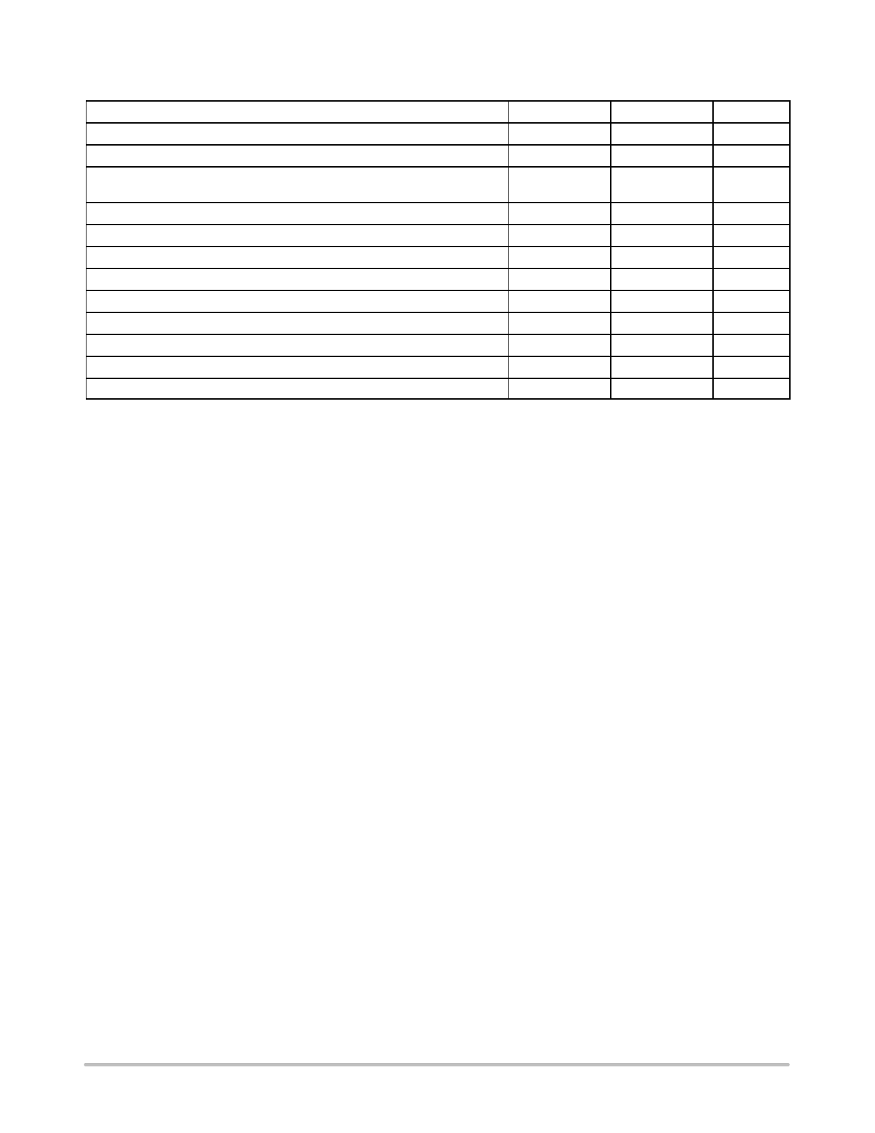
MAXIMUM RATINGS
Rating
Symbol
Value
Unit
High Voltage bridge pin, pin 14
Floating supply voltage, ground referenced
High side output voltage
VBRIDGE
−1 to 600
V
VBOOT − VBRIDGE
0 to 20
V
VDRV(HI)
VBRIDGE−0.3 to
V
VBOOT+0.3
Low side output voltage
Allowable output slew rate
Power Supply voltage, pin 12
Maximum voltage, all pins (except pin 11 and 10)
VDRV(LO)
dVBRIDGE/dt
VCC
−
−0.3 to VCC+0.3
50
20
−0.3 to 10
V
V/ns
V
V
Thermal Resistance Junction−to−Air, PDIP version
Thermal Resistance Junction−to−Air, SOIC version
Storage Temperature Range
RqJA
RqJA
−
100
130
−60 to +150
°C/W
°C/W
°C
ESD Capability, Human Body Model (HBM) (All pins except HV pins)
−
2
kV
ESD Capability, Machine Model (MM)
−
200
V
Stresses exceeding Maximum Ratings may damage the device. Maximum Ratings are stress ratings only. Functional operation above the
Recommended Operating Conditions is not implied. Extended exposure to stresses above the Recommended Operating Conditions may affect
device reliability.
1. This device(s) contains ESD protection and exceeds the following tests:
Human Body Model 2000 V per JEDEC Standard JESD22−A114E
Machine Model 200 V per JEDEC Standard JESD22−A115−A
2. This device meets latchup tests defined by JEDEC Standard JESD78.
http://onsemi.com
5
Share Link: