NCV4264-2 Ver la hoja de datos (PDF) - ON Semiconductor
Número de pieza
componentes Descripción
Lista de partido
NCV4264-2 Datasheet PDF : 11 Pages
| |||
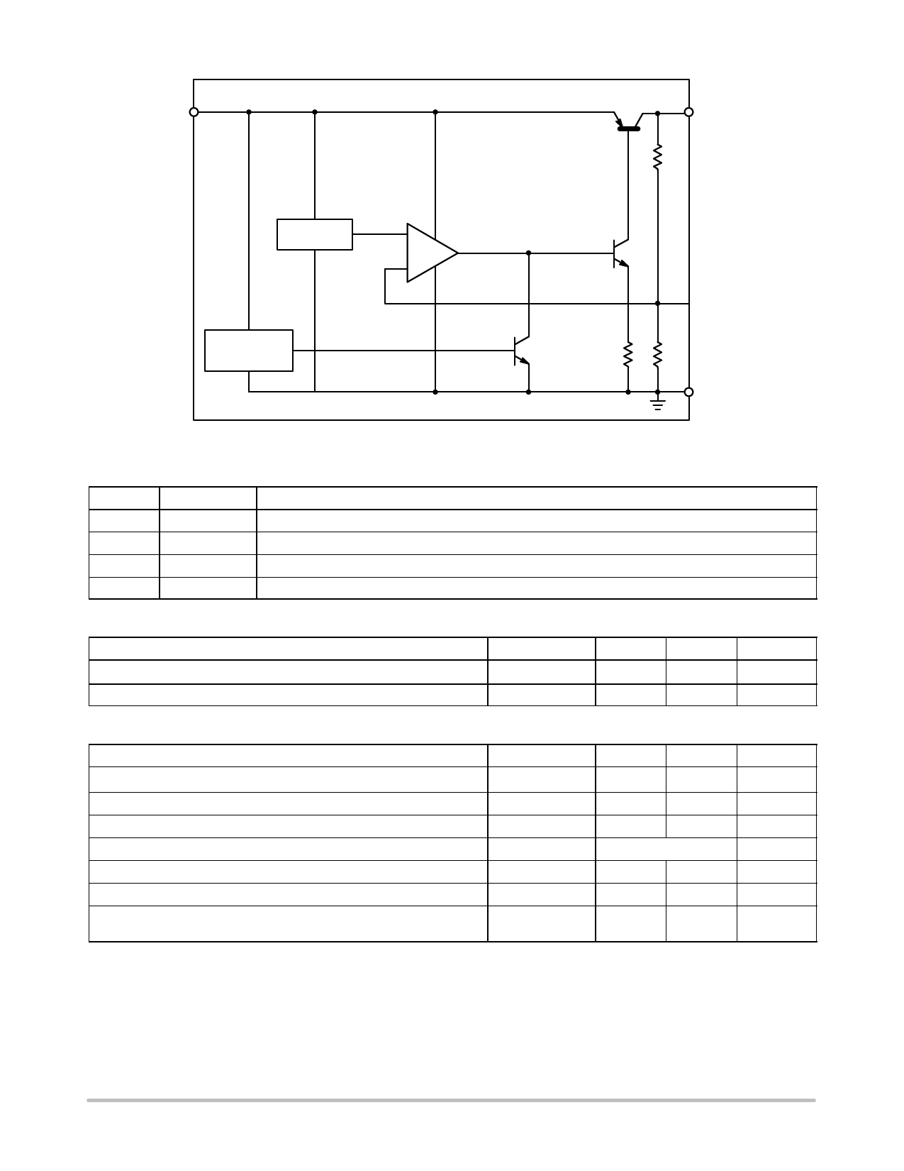
NCV4264-2
IN
OUT
1.3 V
Reference
+
Error
Amp
-
Thermal
Shutdown
GND
Figure 1. Block Diagram
PIN FUNCTION DESCRIPTION
Pin No.
Symbol
Function
1
VIN
Unregulated input voltage; 4.5 V to 45 V.
2
GND
Ground; substrate.
3
VOUT
Regulated output voltage; collector of the internal PNP pass transistor.
TAB
GND
Ground; substrate and best thermal connection to the die.
OPERATING RANGE
Rating
VIN, DC Input Operating Voltage
Junction Temperature Operating Range
Symbol
VIN
TJ
Min
Max
Unit
4.5
+45
V
-40
+150
°C
MAXIMUM RATINGS
Rating
Symbol
Min
Max
Unit
VIN, DC Input Voltage
VOUT, DC Voltage
Storage Temperature
Moisture Sensitivity Level
VIN
VOUT
Tstg
MSL
-42
+45
V
-0.3
+18
V
-55
+150
°C
3
-
ESD Capability, Human Body Model (Note 1)
ESD Capability, Machine Model (Note 1)
Lead Temperature Soldering
Reflow (SMD Styles Only), Lead Free (Note 2)
VESDHB
4000
-
V
VESDMIM
200
-
V
Tsld
°C
-
265 pk
Stresses exceeding Maximum Ratings may damage the device. Maximum Ratings are stress ratings only. Functional operation above the
Recommended Operating Conditions is not implied. Extended exposure to stresses above the Recommended Operating Conditions may affect
device reliability.
1. This device series incorporates ESD protection and is tested by the following methods:
ąESD HBM tested per AEC-Q100-002 (EIA/JESD22-A 114C)
ąESD MM tested per AEC-Q100-003 (EIA/JESD22-A 115C)
2. Lead Free, 60 sec – 150 sec above 217°C, 40 sec max at peak.
http://onsemi.com
2
Share Link: 