NCV4266 Ver la hoja de datos (PDF) - ON Semiconductor
Número de pieza
componentes Descripción
Lista de partido
NCV4266 Datasheet PDF : 11 Pages
| |||
NCV4266
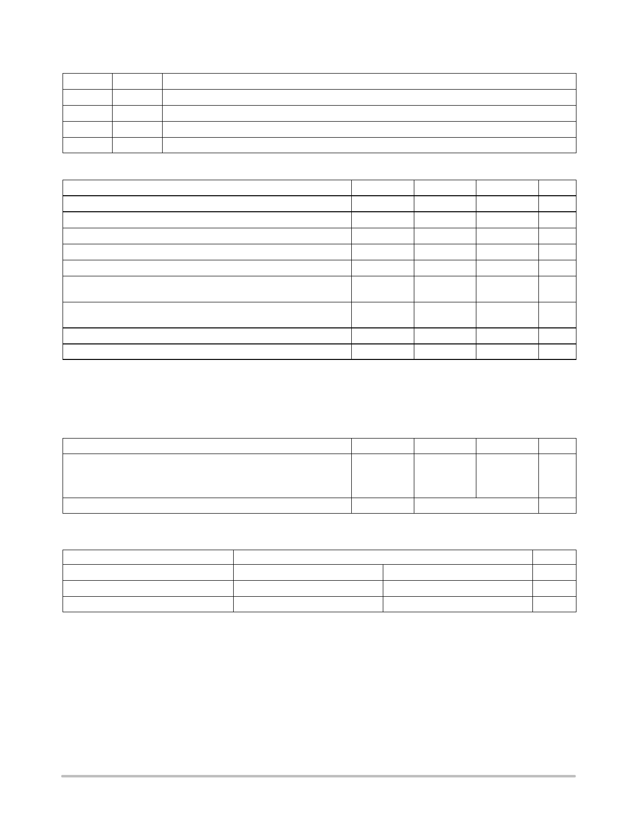
PIN FUNCTION DESCRIPTION
Pin No. Symbol
1
I
Input; Battery Supply Input Voltage.
2
EN
Enable Input; low level disables the IC.
3
Q
Output; Bypass with a capacitor to GND.
4
GND
Ground.
Description
MAXIMUM RATINGS*
Rating
Symbol
Min
Max
Unit
Input Voltage
Input Peak Transient Voltage
Enable Input Voltage
Output Voltage
Ground Current
Input Voltage Operating Range
VI
−42
45
V
VI
−
45
V
VEN
−42
45
V
VQ
−1.0
40
V
Iq
−
100
mA
VI
VQ + 0.5 V or
40
V
4.5 (Note 1)
ESD Susceptibility
(Human Body Model)
−
4.0
−
kV
(Machine Model)
−
250
−
V
Junction Temperature
TJ
−40
150
°C
Storage Temperature
Tstg
−50
150
°C
Stresses exceeding Maximum Ratings may damage the device. Maximum Ratings are stress ratings only. Functional operation above the
Recommended Operating Conditions is not implied. Extended exposure to stresses above the Recommended Operating Conditions may affect
device reliability.
*During the voltage range which exceeds the maximum tested voltage of I, operation is assured, but not specified. Wider limits may apply. Thermal
dissipation must be observed closely.
1. Minimum VI = 4.5 V or (VQ + 0.5 V), whichever is higher.
LEAD TEMPERATURE SOLDERING REFLOW AND MSL (Note 2)
Rating
Symbol
Min
Max
Unit
Lead Temperature Soldering
TSLD
Reflow (SMD styles only), Leaded, 60−150 s above 183, 30 s max at peak
−
Reflow (SMD styles only), Free, 60−150 s above 217, 40 s max at peak
−
Wave Solder (through hole styles only), 12 sec max
−
°C
240
265
310
Moisture Sensitivity Level
2. Per IPC / JEDEC J−STD−020C.
MSL
3
−
THERMAL CHARACTERISTICS
Characteristic
Test Conditions (Typical Value)
Unit
Min Pad Board (Note 3)
1, Pad Board (Note 4)
Junction−to−Tab (psi−JL4, yJL4)
15.7
Junction−to−Ambient (RqJA, qJA)
96
3. 1 oz. copper, 0.26 inch2 (168 mm2) copper area, 0.062″ thick FR4.
4. 1 oz. copper, 1.14 inch2 (736 mm2) copper area, 0.062″ thick FR4.
18
C/W
77
C/W
http://onsemi.com
2
Share Link: 