NCV4269A Ver la hoja de datos (PDF) - ON Semiconductor
Número de pieza
componentes Descripción
Lista de partido
NCV4269A Datasheet PDF : 20 Pages
| |||
NCV4269A
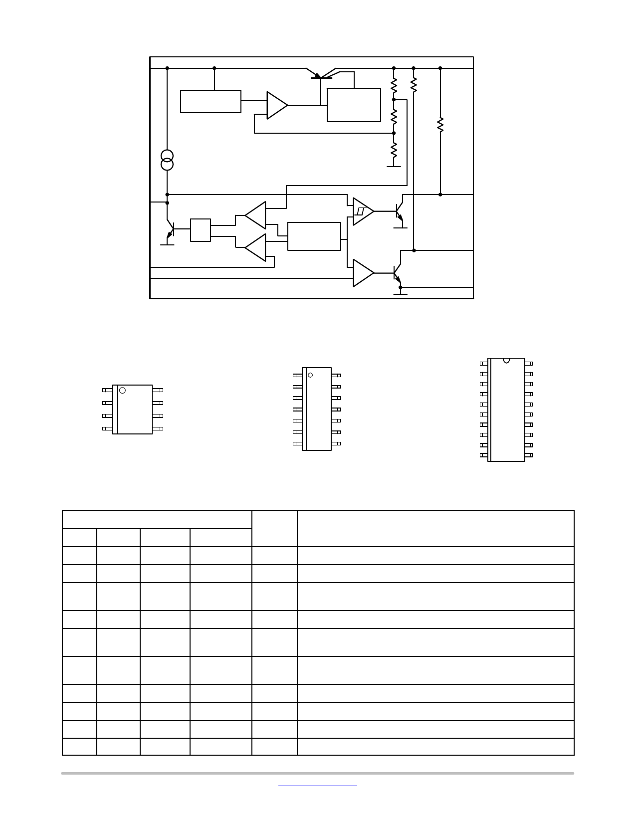
I
Error
Amplifier
Reference
and Trim
Current and
Saturation
Control
Q
RSO
RRO
D
or
RADJ
SI
Reference
+
−
Figure 1. Block Diagram
RO
SO
GND
1
I
SI
RADJ
D
8
Q
SO
RO
GND
SO−8
PIN CONNECTIONS
1
RADJ
D
GND
GND
GND
GND
RO
14
SI
I
GND
GND
GND
Q
SO
SO−14
1
RADJ
D
NC
GND
GND
GND
GND
NC
NC
RO
20
SI
I
NC
GND
GND
GND
GND
NC
Q
SO
SO−20L
PACKAGE PIN DESCRIPTION
Package Pin Number
SO−8 SO−8 EP SO−14
SO−20L
3
3
1
1
4
4
2
2
Pin
Symbol
RADJ
D
Function
Reset Threshold Adjust; if not used to connect to GND.
Reset Delay; To Set Time Delay, Connect to GND with Capacitor
5
5
3, 4, 5, 6, 4, 5, 6, 7, 14, GND Ground
10, 11, 12 15, 16, 17
−
−
−
3, 8, 9, 13, 18
NC
No connection to these pins from the IC.
6
6
7
10
RO
Reset Output; The Open−Collector Output has a 20 kW Pullup Resistor
to Q. Leave Open if Not Used.
7
7
8
11
SO
Sense Output; This Open−Collector Output is Internally Pulled Up by
20 kW pullup resistor to Q. If not used, keep open.
8
8
9
12
Q
5 V or 3.3 V Output; Connect to GND with a 10 mF Capacitor, ESR < 5 W
1
1
13
19
I
Input; Connect to GND Directly at the IC with a Ceramic Capacitor.
2
2
14
20
SI
Sense Input; If not used, Connect to Q.
−
EPAD
−
−
EPAD Connect to ground potential or leave unconnected
www.onsemi.com
2
Share Link: 