NCV4269 Ver la hoja de datos (PDF) - ON Semiconductor
Número de pieza
componentes Descripción
Lista de partido
NCV4269
ON Semiconductor

NCV4269 Datasheet PDF : 16 Pages
| |||
NCV4269
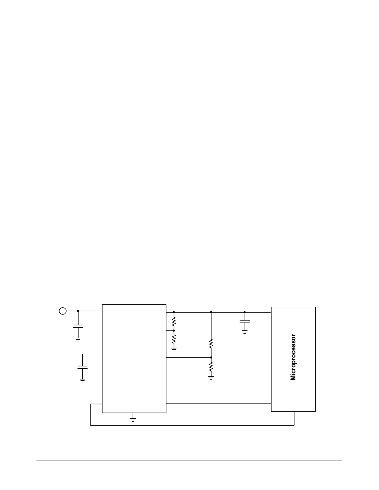
APPLICATION DESCRIPTION
OUTPUT REGULATOR
The output is controlled by a precision trimmed reference.
The PNP output has base drive quiescent current control for
regulation while the input voltage is low, preventing over
saturation. Current limit and voltage monitors complement
the regulator design to give safe operating signals to the
processor and control circuits.
RESET OUTPUT (RO)
A reset signal, Reset Output, RO, (low voltage) is
generated as the IC powers up. After the output voltage VQ
increases above the reset threshold voltage VRT, the delay
timer D is started. When the voltage on the delay timer VD
passes VUD, the reset signal RO goes high. A discharge of
the delay timer VD is started when VQ drops and stays below
the reset threshold voltage VRT. When the voltage of the
delay timer VD drops below the lower threshold voltage VLD
the reset output voltage VRO is brought low to reset the
processor.
The reset output RO is an open collector NPN transistor
with an internal 20 kW pullup resistor connected to the
output Q, controlled by a low voltage detection circuit. The
circuit is functionally independent of the rest of the IC,
thereby guaranteeing that RO is valid for VQ as low as 1.0 V.
RESET ADJUST (RADJ)
The reset threshold VRT can be decreased from a typical
value of 4.65 V to as low as 3.5 V by using an external
voltage divider connected from the Q lead to the pin RADJ,
as shown in Figure 21. The resistor divider keeps the voltage
above the VRADJ,TH (typical 1.35 V) for the desired input
voltages, and overrides the internal threshold detector.
Adjust the voltage divider according to the following
relationship:
VRT + VRADJ, TH @ (RADJ1 ) RADJ2) ń RADJ2
(eq. 1)
If the reset adjust option is not needed, the RADJ pin
should be connected to GND causing the reset threshold to
go to its default value (typically 4.65 V).
RESET DELAY (D)
The reset delay circuit provides a delay (programmable by
capacitor CD) on the reset output lead RO. The delay lead D
provides charge current ID (typically 6.5 mA) to the external
delay capacitor CD during the following times:
1. During Powerup (once the regulation threshold has
been exceeded).
2. After a reset event has occurred and the device is
back in regulation. The delay capacitor is set to
discharge when the regulation (VRT, reset
threshold voltage) has been violated. When the
delay capacitor discharges to VLD, the reset signal
RO pulls low.
SETTING THE DELAY TIME
The delay time is set by the delay capacitor CD and the
charge current ID. The time is measured by the delay
capacitor voltage charging from the low level of VDSAT to
the higher level VUD. The time delay follows the equation:
td + [CD (VUD * VDSAT)]ńID
(eq. 2)
Example:
Using CD = 100 nF.
Use the typical value for VDSAT = 0.1 V.
Use the typical value for VUD = 1.8 V.
Use the typical value for Delay Charge Current ID = 6.5 mA.
td + [100 nF (1.8 * 0.1 V)] ń 6.5 mA + 26.2 ms (eq. 3)
VBAT
CI*
CD
I
Q
0.1 mF
RADJ
NCV4269
D
SI
RADJ1
RADJ2
RSI1
RSI2
VDD
CQ**
10 mF
SO
RO
GND
I/O
I/O
*CI required if regulator is located far from the power supply filter.
** CQ required for Stability. Cap must operate at minimum temperature expected.
Figure 21. Application Diagram
http://onsemi.com
10
Share Link: