NCV4269DW Ver la hoja de datos (PDF) - ON Semiconductor
Número de pieza
componentes Descripción
Lista de partido
NCV4269DW
ON Semiconductor

NCV4269DW Datasheet PDF : 16 Pages
| |||
NCV4269
SENSE INPUT (SI) / SENSE OUTPUT (SO) VOLTAGE
MONITOR
An on−chip comparator is available to provide early
warning to the microprocessor of a possible reset signal. The
output is from an open collector driver with an internal
20 kW pull up resistor to output Q. The reset signal typically
turns the microprocessor off instantaneously. This can cause
unpredictable results with the microprocessor. The signal
received from the SO pin will allow the microprocessor time
to complete its present task before shutting down. This
function is performed by a comparator referenced to the
band gap voltage. The actual trip point can be programmed
externally using a resistor divider to the input monitor SI
(Figure 21). The values for RSI1 and RSI2 are selected for a
typical threshold of 1.20 V on the SI Pin.
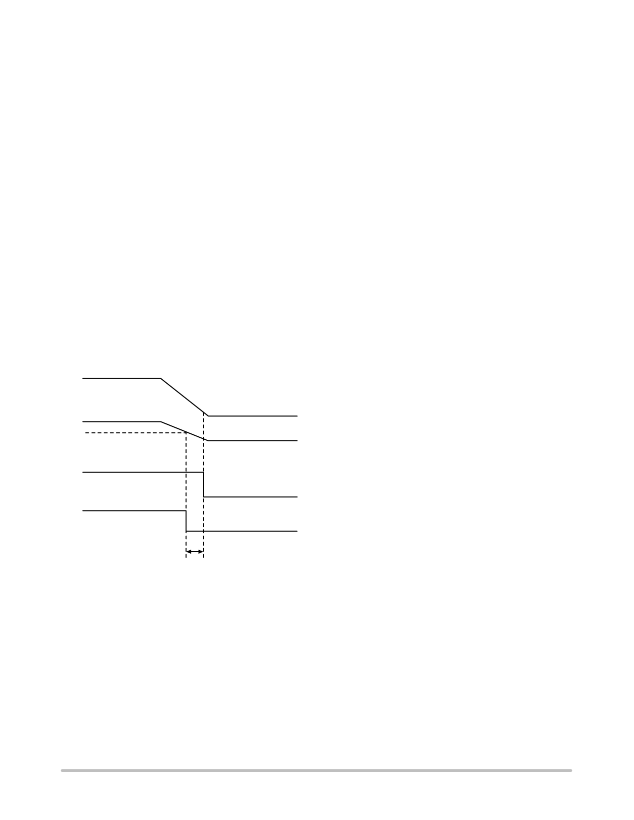
SIGNAL OUTPUT
Figure 22 shows the SO Monitor timing waveforms as a
result of the circuit depicted in Figure 21. As the output
voltage (VQ) falls, the monitor threshold (VSILOW), is
crossed. This causes the voltage on the SO output to go low
sending a warning signal to the microprocessor that a reset
signal may occur in a short period of time. TWARNING is the
time the microprocessor has to complete the function it is
currently working on and get ready for the reset
shutdown signal.
VQ
SI
VSILOW
VRO
SO
TWARNING
Figure 22. SO Warning Waveform Time Diagram
STABILITY CONSIDERATIONS
The input capacitor CI in Figure 21 is necessary for
compensating input line reactance. Possible oscillations
caused by input inductance and input capacitance can be
damped by using a resistor of approximately 1.0 W in series
with CI.
The output or compensation capacitor helps determine
three main characteristics of a linear regulator: startup delay,
load transient response and loop stability.
The capacitor value and type should be based on cost,
availability, size and temperature constraints. A tantalum or
aluminum electrolytic capacitor is best, since a film or
ceramic capacitor with almost zero ESR can cause
instability. The aluminum electrolytic capacitor is the least
expensive solution, but, if the circuit operates at low
temperatures (−25°C to −40°C), both the value and ESR of
the capacitor will vary considerably. The capacitor
manufacturer’s data sheet usually provides this information.
The value for the output capacitor CQ shown in Figure 21
should work for most applications; however, it is not
necessarily the optimized solution. Stability is guaranteed at
values CQ = 10 mF and an ESR = 10 W within the operating
temperature range. Actual limits are shown in a graph in the
typical data section.
CALCULATING POWER DISSIPATION IN A SINGLE
OUTPUT LINEAR REGULATOR
The maximum power dissipation for a single output
regulator (Figure 21) is:
PD(max) + [VI(max) * VQ(min)] IQ(max) ) VI(max) Iq (eq. 4)
where:
VI(max) is the maximum input voltage,
VQ(min) is the minimum output voltage,
IQ(max) is the maximum output current for the application,
and Iq is the quiescent current the regulator consumes at
IQ(max).
Once the value of PD(max) is known, the maximum
permissible value of RqJA can be calculated:
RqJA = (150°C – TA) / PD
(eq. 5)
The value of RqJA can then be compared with those in the
package section of the data sheet. Those packages with
RqJA’s less than the calculated value in equation 2 will keep
the die temperature below 150°C. In some cases, none of the
packages will be sufficient to dissipate the heat generated by
the IC, and an external heatsink will be required. The current
flow and voltages are shown in the
Measurement Circuit Diagram.
HEATSINKS
A heatsink effectively increases the surface area of the
package to improve the flow of heat away from the IC and
into the surrounding air.
Each material in the heat flow path between the IC and the
outside environment will have a thermal resistance. Like
series electrical resistances, these resistances are summed to
determine the value of RqJA:
RqJA + RqJC ) RqCS ) RqSA
(eq. 6)
where:
RqJC = the junction−to−case thermal resistance,
RqCS = the case−to−heat sink thermal resistance, and
RqSA = the heat sink−to−ambient thermal resistance.
RqJC appears in the package section of the data sheet. Like
RqJA, it too is a function of package type. RqCS and RqSA are
functions of the package type, heatsink and the interface
between them. These values appear in data sheets of
heatsink manufacturers. Thermal, mounting, and
heatsinking considerations are discussed in the
ON Semiconductor application note AN1040/D, available
on the ON Semiconductor website.
http://onsemi.com
11
Share Link: