NCV8664 Ver la hoja de datos (PDF) - ON Semiconductor
Número de pieza
componentes Descripción
Lista de partido
NCV8664 Datasheet PDF : 18 Pages
| |||
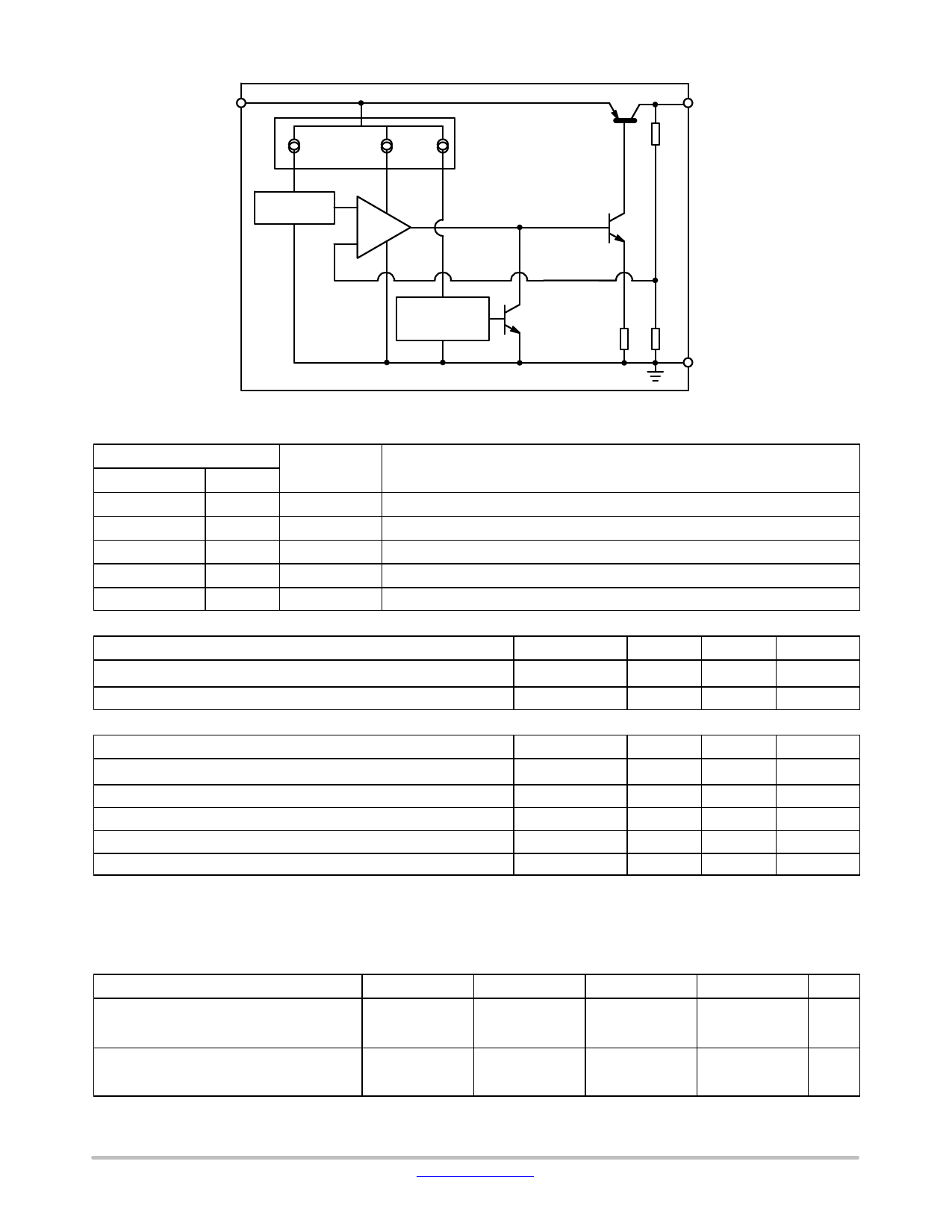
IN
Bias Current
Generators
1.3 V
Reference
+
Error
Amp
-
NCV8664
OUT
Thermal
Shutdown
GND
Figure 1. Block Diagram
PIN FUNCTION DESCRIPTION
Pin No.
DPAK/SOT−223 SOIC−8
Symbol
Function
1
2
VIN
Unregulated input voltage; 4.5 V to 45 V.
2
3
GND
Ground; substrate.
3
4
VOUT
Regulated output voltage; collector of the internal PNP pass transistor.
TAB
−
GND
Ground; substrate and best thermal connection to the die.
−
1, 5−8
NC
No Connection.
OPERATING RANGE
Pin Symbol, Parameter
Symbol
Min
Max
Unit
VIN, DC Input Operating Voltage
Junction Temperature Operating Range
MAXIMUM RATINGS
VIN
4.5
+45
V
TJ
−40
+150
°C
Rating
Symbol
Min
Max
Unit
VIN, DC Voltage
VIN
−42
+45
V
VOUT, DC Voltage
VOUT
−0.3
+18
V
Storage Temperature
Tstg
−55
+150
°C
ESD Capability, Human Body Model (Note 1)
VESDHB
4000
−
V
ESD Capability, Machine Model (Note 1)
VESDMIM
200
−
V
Stresses exceeding those listed in the Maximum Ratings table may damage the device. If any of these limits are exceeded, device functionality
should not be assumed, damage may occur and reliability may be affected.
1. This device series incorporates ESD protection and is tested by the following methods:
ESD HBM tested per AEC−Q100−002 (EIA/JESD22−A 114C)
ESD MM tested per AEC−Q100−003 (EIA/JESD22−A 115C)
THERMAL RESISTANCE
Parameter
Symbol
Condition
Min
Max
Unit
Junction−to−Ambient
DPAK
SOT−223
SOIC−8 Fused
RqJA
−
101 (Note 2)
°C/W
−
99 (Note 2)
−
145
Junction−to−Case
DPAK
SOT−223
SOIC−8 Fused
RqJC
−
9.0
°C/W
−
17
−
−
2. 1 oz., 100 mm2 copper area.
www.onsemi.com
2
Share Link: 