NCV8665 Ver la hoja de datos (PDF) - ON Semiconductor
Número de pieza
componentes Descripción
Lista de partido
NCV8665 Datasheet PDF : 13 Pages
| |||
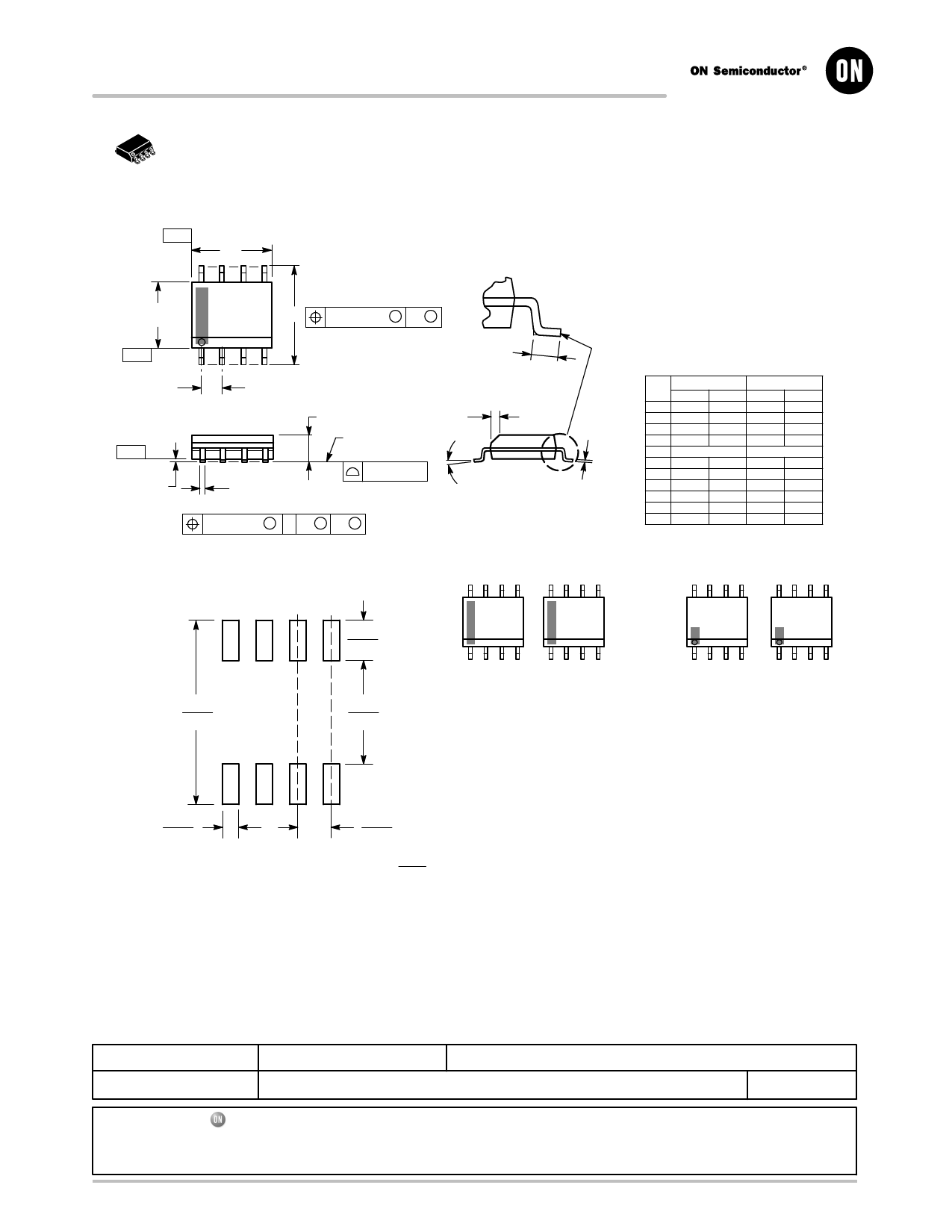
MECHANICAL CASE OUTLINE
PACKAGE DIMENSIONS
8
1
SCALE 1:1
SOIC−8 NB
CASE 751−07
ISSUE AK
DATE 16 FEB 2011
−X−
A
B
−Y−
−Z−
H
8
5
S
0.25 (0.010) M Y M
1
4
K
G
D
C
SEATING
PLANE
N X 45 _
0.10 (0.004)
M
0.25 (0.010) M Z Y S X S
NOTES:
1. DIMENSIONING AND TOLERANCING PER
ANSI Y14.5M, 1982.
2. CONTROLLING DIMENSION: MILLIMETER.
3. DIMENSION A AND B DO NOT INCLUDE
MOLD PROTRUSION.
4. MAXIMUM MOLD PROTRUSION 0.15 (0.006)
PER SIDE.
5. DIMENSION D DOES NOT INCLUDE DAMBAR
PROTRUSION. ALLOWABLE DAMBAR
PROTRUSION SHALL BE 0.127 (0.005) TOTAL
IN EXCESS OF THE D DIMENSION AT
MAXIMUM MATERIAL CONDITION.
6. 751−01 THRU 751−06 ARE OBSOLETE. NEW
STANDARD IS 751−07.
MILLIMETERS
INCHES
DIM MIN MAX MIN MAX
A 4.80 5.00 0.189 0.197
B 3.80 4.00 0.150 0.157
C 1.35 1.75 0.053 0.069
D 0.33 0.51 0.013 0.020
G
1.27 BSC
0.050 BSC
H 0.10 0.25 0.004 0.010
J 0.19 0.25 0.007 0.010
J
K 0.40 1.27 0.016 0.050
M
0_ 8_ 0_ 8_
N 0.25 0.50 0.010 0.020
S 5.80 6.20 0.228 0.244
SOLDERING FOOTPRINT*
1.52
0.060
7.0
0.275
4.0
0.155
GENERIC
MARKING DIAGRAM*
8
XXXXX
ALYWX
1
IC
8
XXXXX
ALYWX
G
1
IC
(Pb−Free)
8
XXXXXX
AYWW
1
Discrete
8
XXXXXX
AYWW
G
1
Discrete
(Pb−Free)
XXXXX = Specific Device Code
A
= Assembly Location
L
= Wafer Lot
Y
= Year
W
= Work Week
G
= Pb−Free Package
XXXXXX = Specific Device Code
A
= Assembly Location
Y
= Year
WW = Work Week
G
= Pb−Free Package
0.6
0.024
1.270
0.050
ǒ Ǔ SCALE 6:1
mm
inches
*For additional information on our Pb−Free strategy and soldering
details, please download the ON Semiconductor Soldering and
Mounting Techniques Reference Manual, SOLDERRM/D.
*This information is generic. Please refer to
device data sheet for actual part marking.
Pb−Free indicator, “G” or microdot “G”, may
or may not be present. Some products may
not follow the Generic Marking.
STYLES ON PAGE 2
DOCUMENT NUMBER: 98ASB42564B
DESCRIPTION: SOIC−8 NB
Electronic versions are uncontrolled except when accessed directly from the Document Repository.
Printed versions are uncontrolled except when stamped “CONTROLLED COPY” in red.
PAGE 1 OF 2
ON Semiconductor and
are trademarks of Semiconductor Components Industries, LLC dba ON Semiconductor or its subsidiaries in the United States and/or other countries.
ON Semiconductor reserves the right to make changes without further notice to any products herein. ON Semiconductor makes no warranty, representation or guarantee regarding
the suitability of its products for any particular purpose, nor does ON Semiconductor assume any liability arising out of the application or use of any product or circuit, and specifically
disclaims any and all liability, including without limitation special, consequential or incidental damages. ON Semiconductor does not convey any license under its patent rights nor the
rights of others.
© Semiconductor Components Industries, LLC, 2019
www.onsemi.com
Share Link: 