NCV8674(2008) Ver la hoja de datos (PDF) - ON Semiconductor
Número de pieza
componentes Descripción
Lista de partido
NCV8674 Datasheet PDF : 11 Pages
| |||
NCV8674
Circuit Description
The NCV8674 is a precision trimmed 5.0 V or 12 V fixed
output regulator. Careful management of light load
consumption combined with a low leakage process results
in a typical quiescent current of 30 mA. The device has
current capability of 350 mA, with 600 mV of dropout
voltage at full rated load current. The regulation is provided
by a PNP pass transistor controlled by an error amplifier
with a bandgap reference. The regulator is protected by
both current limit and short circuit protection. Thermal
shutdown occurs above 150°C to protect the IC during
overloads and extreme ambient temperatures.
Regulator
The error amplifier compares the reference voltage to a
sample of the output voltage (Vout) and drives the base of
a PNP series pass transistor by a buffer. The reference is a
bandgap design to give it a temperature−stable output.
Saturation control of the PNP is a function of the load
current and input voltage. Over saturation of the output
power device is prevented, and quiescent current in the
ground pin is minimized. The NCV8674 is equipped with
foldback current protection. This protection is designed to
reduce the current limit during an overcurrent situation.
Regulator Stability Considerations
The input capacitor CIN in Figure 2 is necessary for
compensating input line reactance. Possible oscillations
caused by input inductance and input capacitance can be
damped by using a resistor of approximately 1 W in series
with CIN. The output or compensation capacitor, COUT
helps determine three main characteristics of a linear
regulator: startup delay, load transient response and loop
stability. The capacitor value and type should be based on
cost, availability, size and temperature constraints.
Tantalum, aluminum electrolytic, film, or ceramic
capacitors are all acceptable solutions, however, attention
must be paid to ESR constraints. The aluminum
electrolytic capacitor is the least expensive solution, but, if
the circuit operates at low temperatures (−25°C to −40°C),
both the value and ESR of the capacitor will vary
considerably. The capacitor manufacturer’s data sheet
usually provides this information. The value for the output
capacitor COUT shown in Figure 2 should work for most
applications; however, it is not necessarily the optimized
solution. Stability is guaranteed at values COUT ≥ 22 mF and
ESR ≤ 7.0 W, within the operating temperature range.
Actual limits are shown in a graph in the Typical
Characteristics section.
Calculating Power Dissipation in a Single Output
Linear Regulator
The maximum power dissipation for a single output
regulator (Figure 2) is:
PD(max) + [VIN(max) * VOUT(min)] @
IOUT(max) ) VIN(max) @ Iq (eq. 1)
Where:
VIN(max) is the maximum input voltage,
VOUT(min) is the minimum output voltage,
IOUT(max) is the maximum output current for the
application, and Iq is the quiescent current the regulator
consumes at IOUT(max).
Once the value of PD(Max) is known, the maximum
permissible value of RqJA can be calculated:
RqJA
+
150oC *
PD
TA
(eq. 2)
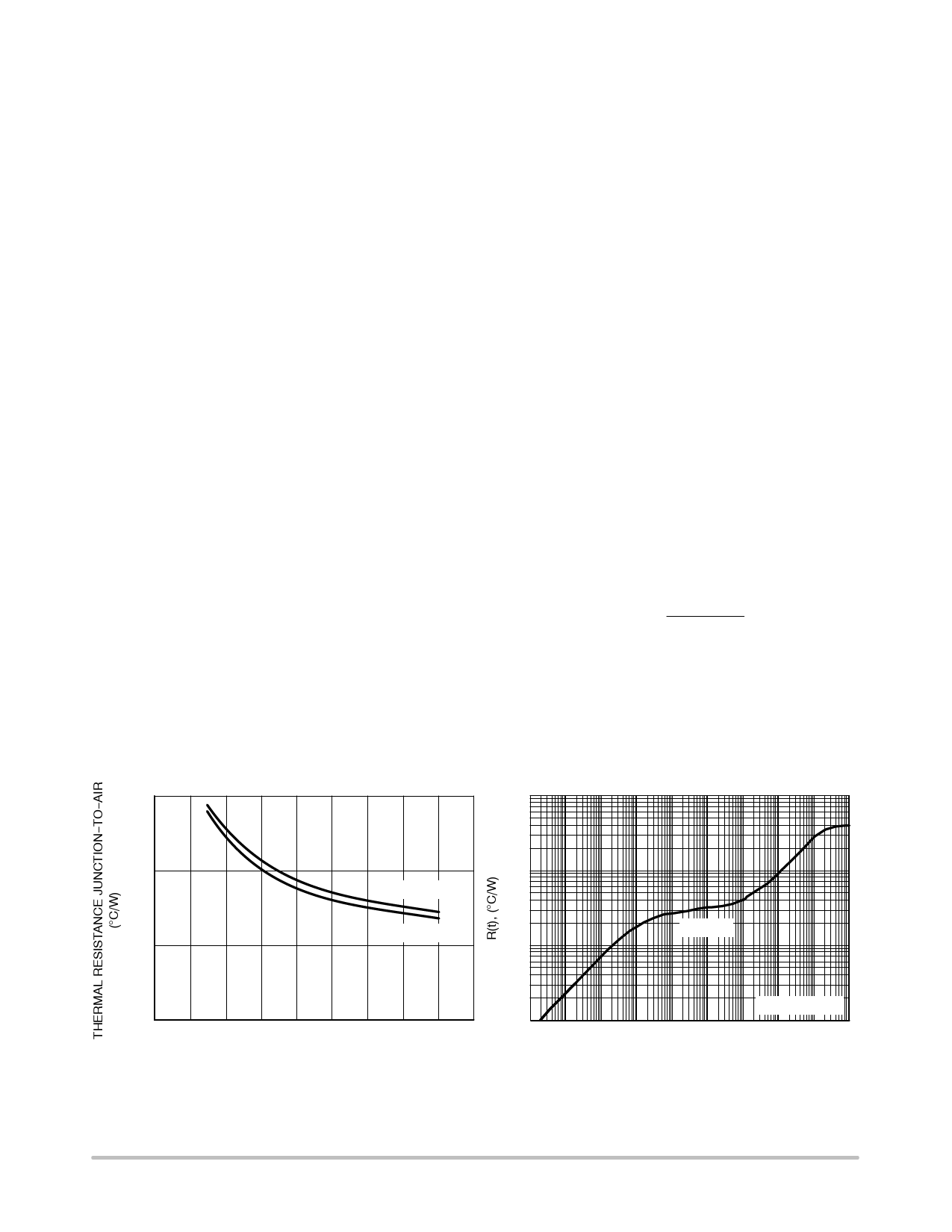
The value of RqJA can then be compared with those in
thermal resistance versus copper area graph (Figure 26).
Those designs with cooling area corresponding to RqJA’s
less than the calculated value in Equation 2 will keep the
die temperature below 150°C. The current flow and
voltages are shown in the Measurement Circuit Diagram.
75
100
50
10
D2PAK 1 oz
D2PAK 2 oz
D2PAK
25
1
0
0.1
0 100 200 300 400 500 600 700 800 900 0.000001
0.0001
0.01 0.1
Single Pulse
1 10 100 1000
COPPER AREA (mm2)
PULSE TIME (sec)
Figure 26.
Figure 27. NCV8674 @ PCB Cu Area 650 mm2
PCB Cu thk 1 oz
http://onsemi.com
9
Share Link: 