NCV8674DS120G Ver la hoja de datos (PDF) - ON Semiconductor
Número de pieza
componentes Descripción
Lista de partido
NCV8674DS120G Datasheet PDF : 12 Pages
| |||
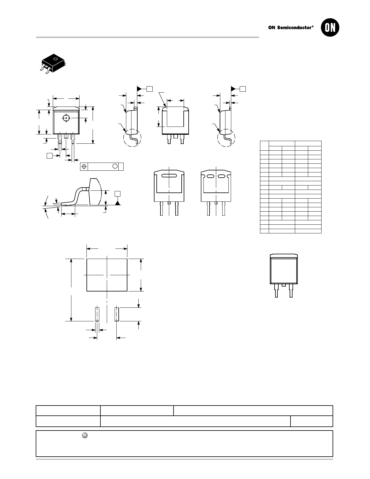
MECHANICAL CASE OUTLINE
PACKAGE DIMENSIONS
D2PAK
CASE 936−03
ISSUE E
SCALE 1:1
K
A
T
T
TERMINAL 4
C
C
OPTIONAL
CHAMFER
ED
U
OPTIONAL
CHAMFER
ES
S
B
H DETAIL C
12 3
V
DETAIL C
J
F
G
2X D
SIDE VIEW
DUAL GAUGE
CONSTRUCTION
TOP VIEW 0.010 (0.254) M T
BOTTOM VIEW
SIDE VIEW
SINGLE GAUGE
CONSTRUCTION
N
R
T
M
P
L
DETAIL C
SEATING
PLANE
BOTTOM VIEW
OPTIONAL CONSTRUCTIONS
DATE 29 SEP 2015
NOTES:
1. DIMENSIONING AND TOLERANCING PER ANSI
Y14.5M, 1982.
2. CONTROLLING DIMENSION: INCHES.
3. TAB CONTOUR OPTIONAL WITHIN DIMENSIONS
A AND K.
4. DIMENSIONS U AND V ESTABLISH A MINIMUM
MOUNTING SURFACE FOR TERMINAL 4.
5. DIMENSIONS A AND B DO NOT INCLUDE MOLD
FLASH OR GATE PROTRUSIONS. MOLD FLASH
AND GATE PROTRUSIONS NOT TO EXCEED
0.025 (0.635) MAXIMUM.
6. SINGLE GAUGE DESIGN WILL BE SHIPPED AF
TER FPCN EXPIRATION IN OCTOBER 2011.
INCHES
MILLIMETERS
DIM MIN MAX MIN MAX
A 0.386 0.403 9.804 10.236
B 0.356 0.368 9.042 9.347
C 0.170 0.180 4.318 4.572
D 0.026 0.036 0.660 0.914
ED 0.045 0.055
ES 0.018 0.026
F 0.051 REF
1.143 1.397
0.457 0.660
1.295 REF
G 0.100 BSC
2.540 BSC
H 0.539 0.579 13.691 14.707
J 0.125 MAX
3.175 MAX
K 0.050 REF
1.270 REF
L 0.000 0.010 0.000 0.254
M 0.088 0.102 2.235 2.591
N 0.018 0.026 0.457 0.660
P 0.058 0.078 1.473 1.981
R
0_
8_
0_
8_
S
0.116 REF
2.946 REF
U
0.200 MIN
5.080 MIN
V
0.250 MIN
6.350 MIN
SOLDERING FOOTPRINT*
10.490
GENERIC
MARKING DIAGRAM*
16.155
8.380
2X
3.504
2X 1.016
5.080
PITCH
DIMENSIONS: MILLIMETERS
*For additional information on our Pb−Free strategy and soldering
details, please download the ON Semiconductor Soldering and
Mounting Techniques Reference Manual, SOLDERRM/D.
XXXXXXG
ALYWW
XXXXXX = Specific Device Code
A
= Assembly Location
L
= Wafer Lot
Y
= Year
WW = Work Week
G
= Pb−Free Package
*This information is generic. Please refer to
device data sheet for actual part marking.
Pb−Free indicator, “G” or microdot “ G”,
may or may not be present.
DOCUMENT NUMBER: 98ASH01005A
DESCRIPTION: D2PAK
Electronic versions are uncontrolled except when accessed directly from the Document Repository.
Printed versions are uncontrolled except when stamped “CONTROLLED COPY” in red.
PAGE 1 OF 1
ON Semiconductor and
are trademarks of Semiconductor Components Industries, LLC dba ON Semiconductor or its subsidiaries in the United States and/or other countries.
ON Semiconductor reserves the right to make changes without further notice to any products herein. ON Semiconductor makes no warranty, representation or guarantee regarding
the suitability of its products for any particular purpose, nor does ON Semiconductor assume any liability arising out of the application or use of any product or circuit, and specifically
disclaims any and all liability, including without limitation special, consequential or incidental damages. ON Semiconductor does not convey any license under its patent rights nor the
rights of others.
© Semiconductor Components Industries, LLC, 2019
www.onsemi.com
Share Link: 