NJM2801U Ver la hoja de datos (PDF) - Japan Radio Corporation
Número de pieza
componentes Descripción
Lista de partido
NJM2801U Datasheet PDF : 4 Pages
| |||
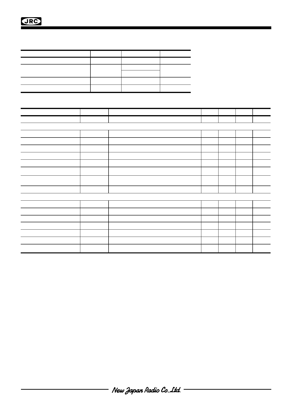
■ Absolute Maximum Ratings
PARAMETER
Input Voltage
Power Dissipation
Operating
Temperature
Storage Temperature Range
SYMBOL
VIN
PD
Topr
Tstg
(Ta=25°C)
RATINGS
UNIT
+14
V
200 (MTP5)
350 (SOT-89)
mW
−40∼+85
°C
−40∼+125
°C
NJM2801
PRELIMINARY
■ ELECTRICAL CHARACTERISTICS (VIN=Vo+1V , CIN=0.1µF, Co=1µF ( Vo≤2.6V: Co=2.2µF ) Ta=25°C )
PARAMETER
SYMBOL
CONDITION
MIN. TYP. MAX. UNIT
Quiescent Current
Regulator Block
IQ
Io=0mA
−
200 300 µA
Output Voltage
Vo
Io=30mA
-2.2% − +2.2% V
Output Current
Io
Vo-0.3V
150 200
−
mA
Line Regulation
Load Regulation
Dropout Voltage
∆Vo/∆VIN
∆Vo/∆Io
∆VI_O
VIN=Vo+1V∼Vo+6V, Io=30mA
Io=0∼100mA
Io=60mA
−
− 0.10 %/V
−
− 0.03 %/mA
− 0.10 0.18 V
Ripple Rejection
RR
Ein=200mVrms, f=1kHz, Io=10mA,Vo=3V −
60
−
dB
Output
Voltage
Temperature Coefficient
Output Noise Voltage
∆Vo/∆T
VNO
Ta=0∼85°C, Io=10mA
f=10Hz∼100kHz, Io=10mA, Vo=3V
−
±50
− ppm/°C
−
45
− µVrms
Reset Block
Voltage Detection
Hysteresis Voltage
Low Level Output
Output Leak Current
On time Output Current
Reset Output Delay
Operation Voltage Limit
VRT
VRTH
RORL
IORH
IORL
td
VOPL
VIN=H→L
−2% − +2% V
VIN=H→L→H
VRT×3% VRT×5% VRT×8% mV
VIN=VRT-0.5V, RL=100kΩ
− 100 300 mV
VIN= VRT-0.5V
−
−
0.1 µA
VIN=VRT-0.5V, RL=0Ω
5
−
−
mA
VIN=(VRT-0.5V)→ (VRT+0.5V), Cd=0.1µF
9
10
11
mS
VORL=0.4V
−
0.9
−
V
The above specification is a common specification for all output voltages.
Therefore, it may be different from individual specification for a specific output voltage.
Share Link: 