NJM2807DL2(2003) Ver la hoja de datos (PDF) - Japan Radio Corporation
Número de pieza
componentes Descripción
Lista de partido
NJM2807DL2 Datasheet PDF : 5 Pages
| |||
NJM2807
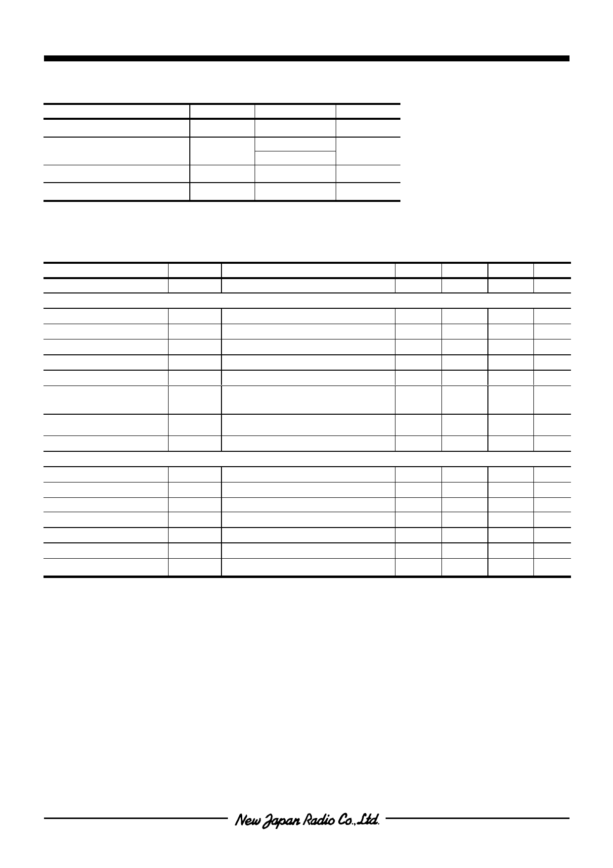
ABSOLUTE MAXIMUM RATINGS
PARAMETER
SYMBOL
Input Voltage
VIN
Power Dissipation
PD
Operating Temperature
Topr
Storage Temperature
Tstg
RATINGS
+14
8 (Tc=25°C)
0.8(Ta≤25°C)
−40∼+85
−40∼+125
(Ta=25°C)
UNIT
V
W
°C
°C
ELECTRICAL CHARACTERISTICS
(VIN=Vo+1V, CIN=0.1µF, Co=2.2µF (Vo≤2.6V: Co=4.7µF) Ta=25°C)
PARAMETER
SYMBOL
TEST CONDITION
MIN. TYP. MAX. UNIT
Quiescent Current
Regulator Block
IQ
VIN=Vo+2V, Io=0mA
−
330 430 µA
Output Voltage
Output Current
Line Regulation
Load Regulation
Dropout Voltage
Vo
Io
∆Vo/∆VIN
∆Vo/∆Io
∆VI_O
Io=30mA
Vo-0.3V
VIN=Vo+1V∼Vo+6V, Io=30mA
Io=0∼500mA
Io=300mA
−1.0% − +1.0% V
500 650
−
mA
−
− 0.10 %/V
−
− 0.03 %/mA
− 0.18 0.28 V
Ripple Rejection
RR
ein=200mVrms, f=1kHz, Io=10mA,Vo=3V Version −
75
−
dB
Output Voltage Temperature
Coefficient
Output Noise Voltage
∆Vo/∆T
VNO
Ta=0∼85°C, Io=10mA
f=10Hz∼100kHz, Io=10mA, Vo=3V Version
−
±50
− ppm/°C
−
45
− µVrms
Reset Block
Voltage Detection
Hysteresis Voltage
Low Level Output Voltage
Output Leak Current
On time Output Current
Reset Output Delay Time
VRT
VRTH
RORL
IORH
IORL
td
VIN=H→L
VIN=H→L→H
VIN=VRT-0.5V, RL=100kΩ
VIN= VRT+0.5V
VIN=VRT-0.5V, RL=0Ω
VIN=(VRT-0.5V)→ (VRT+0.5V), Cd=0.1µF
−1.0% − +1.0% V
VRT×3 VRT×5 VRT×8 mV
−
100 300 mV
−
−
0.1 µA
5
−
−
mA
9
10
11
mS
Operation Voltage Limit
VOPL
VORL=0.4V
−
0.9
−
V
(*note 1) The above specification is a common specification for all output voltages.
Therefore, it may be different from the individual specification for a specific output voltage.
-2-
Ver.2003-11-10
Share Link: 