BS616LV2015 Ver la hoja de datos (PDF) - Brilliance Semiconductor
Número de pieza
componentes Descripción
Lista de partido
BS616LV2015 Datasheet PDF : 11 Pages
| |||
BSI
BS616LV2015
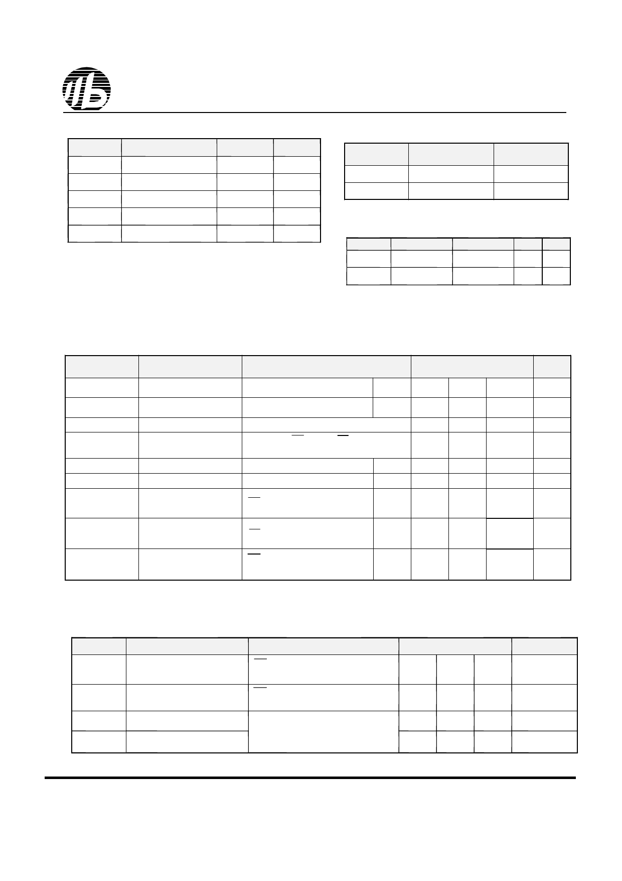
ABSOLUTE MAXIMUM RATINGS(1)
OPERATING RANGE
SYMBOL
V TERM
T BIAS
T STG
PT
I OUT
PARAMETER
Terminal Voltage with
Respect to GND
Temperature Under Bias
Storage Temperature
Power Dissipation
DC Output Current
RATING
-0.5 to
Vcc+0.5
-40 to +125
-60 to +150
1.0
20
UNITS
V
OC
OC
W
mA
1. Stresses greater than those listed under ABSOLUTE MAXIMUM
RATINGS may cause permanent damage to the device. This is a
stress rating only and functional operation of the device at these
or any other conditions above those indicated in the operational
sections of this specification is not implied. Exposure to absolute
maximum rating conditions for extended periods may affect
reliability.
RANGE
Commercial
Industrial
AMBIENT
TEMPERATURE
0 O C to +70 O C
-40 O C to +85 O C
Vcc
4.5V ~ 5.5V
4.5V ~ 5.5V
CAPACITANCE (1) (TA = 25oC, f = 1.0 MHz)
SYMBOL
CIN
CDQ
PARAMETER
Input
Capacitance
Input/Output
Capacitance
CONDITIONS
VIN=0V
VI/O=0V
MAX. UNIT
6 pF
8 pF
1. This parameter is guaranteed and not tested.
DC ELECTRICAL CHARACTERISTICS ( TA = 0 to + 70oC )
PARAMETER
NAME
VIL
VIH
IIL
IOL
VOL
VOH
PARAMETER
Guaranteed Input Low
Voltage(2)
Guaranteed Input High
Voltage(2)
Input Leakage Current
Output Leakage Current
Output Low Voltage
Output High Voltage
TEST CONDITIONS
Vcc=5.0V
Vcc=5.0V
Vcc = Max, VIN = 0V to Vcc
Vcc = Max, CE = VIH, or OE = VIH,
VI/O = 0V to Vcc
Vcc = Max, IOL = 2mA
Vcc=5.0V
Vcc = Min, IOH = -1mA
Vcc=5.0V
ICC
Operating Power Supply
Current
CE = VIL, IDQ = 0mA, F = Fmax(3)
Vcc=5.0V
MIN. TYP. (1) MAX.
UNITS
-0.5
--
0.8
V
2.2
--
Vcc+0.2
V
--
--
1
uA
--
--
1
uA
--
--
0.4
V
2.4
--
--
V
--
--
40
mA
ICCSB
Standby Current-TTL
CE = VIH, IDQ = 0mA
Vcc=5.0V
--
--
1
mA
CE Њ Vcc-0.2V,
ICCSB1
Standby Current-CMOS
Vcc=5.0V
VIN Њ Vcc - 0.2V or VIN Љ 0.2V
--
0.6
6
uA
1. Typical characteristics are at TA = 25oC.
2. These are absolute values with respect to device ground and all overshoots due to system or tester notice are included.
3. Fmax = 1/tRC .
DATA RETENTION CHARACTERISTICS ( TA = 0 to + 70oC )
SYMBOL
PARAMETER
VDR
Vcc for Data Retention
ICCDR
Data Retention Current
tCDR
Chip Deselect to Data
Retention Time
tR
Operation Recovery Time
1. Vcc = 1.5V, TA = + 25OC
2. tRC = Read Cycle Time
R0201-BS616LV2015
TEST CONDITIONS
CE Њ Vcc - 0.2V
VIN Њ Vcc - 0.2V or VIN Љ 0.2V
CE Њ Vcc - 0.2V
VIN Њ Vcc - 0.2V or VIN Љ 0.2V
See Retention Waveform
3
MIN. TYP. (1) MAX.
1.5
--
--
--
0.05
1.5
0
--
--
TRC (2)
--
--
UNITS
V
uA
ns
ns
Revision 2.5
April 2002
Share Link: 