PJ1583CM Ver la hoja de datos (PDF) - Promax Johnton
Número de pieza
componentes Descripción
Lista de partido
PJ1583CM Datasheet PDF : 6 Pages
| |||
PJ1581/PJ1582/PJ1583
Dual Input Low Dropout Voltage Regulator
PIN FUNCTION
Pin 1: SENSE - This pin is the positive side of the reference voltage for this device. With this pin it is possible to Kelvin
Sense the output voltage at the load
Pin 2: ADJUST- This pin is the negative side of the reference voltage for this device. Transient response can be improved
by adding a small bypass capacitor from the adjust pin to ground
Pin 3: OUTPUT- This pin is power output of the device.
Pin 4: CONTROL- This pin is the supply pin for the control circuitry for the device. The current flow into this pin will be
about 1% of the output current. For the device to regulate, the voltage at this pin must be 1.3V greater
than the output voltage.
Pin 5: POWER- This pin is the collector of the power transistor. The output load current is supplied through this pin.
The voltage at this pin must be 0.7V greater than the output voltage for the device to regulate.
APPLICATION INFORMATION
The PJ1581 is a low dropout regulator designed to make used
of multiple power supplies, present in most systems, to reduce
the dropout voltage. One of the advantages of the two supply
approach is maximizing the efficiency. The second supply is
at least 1V greater than output voltage and is providing the
power for the control circuitry and supplies the drive current
to the NPN output transistor. This allows the NPN output
transistor to be driven into saturation. For the control voltage
the current requirement is small equal to about 1% of the
output current or approximately 50mA for a 5A load. This
drive current becomes part of the output current. The
maximum voltage on the Control Pin is 15V. The maximum
voltage at the Power in is 7V.By tying the control and power
inputs together the PJ1581 can also be operated as a single
supply device. In single supply, the minimum control voltage
will determine operation the dropout.
Both the fixed and adjustable versions have remote sense pins,
permitting very accurate regulation of output voltage. As a
result, over and output current range of 100mA to 5A, the
typical load regulation is less than 1mV. For the fixed voltages
the adjust pin is brought out allowing the user to improve
transient response by bypassing the internal resistor divider.
Optimum transient response is provided using a capacitor in
the range of 0.1uF to 1uF for bypassing the adjust pin.
The new generation of microprocessors cycle load current
from several hundred million amperes to several amperes in
tens of nanoseconds. Output voltage tolerances are tighter and
include transient response as part of the specification.
Designed to meet the fast current load step requirements of
these microprocessors, the PJ1581 also saves total cost by
needing less output capacitance to maintain regulation.
Typical applications for the PJ1581 include 3.3V to 2.5V
conversion with a 5V control supply, 5V to 4.2V conversion
with a 12V control supply or 5V to 3.6V conversion with a
12V control supply. It is easy to obtain dropout voltages less
than 0.5V at 2.5A along with excellent static and dynamic
specifications. It is fully protected against over current and
over temperature conditions.
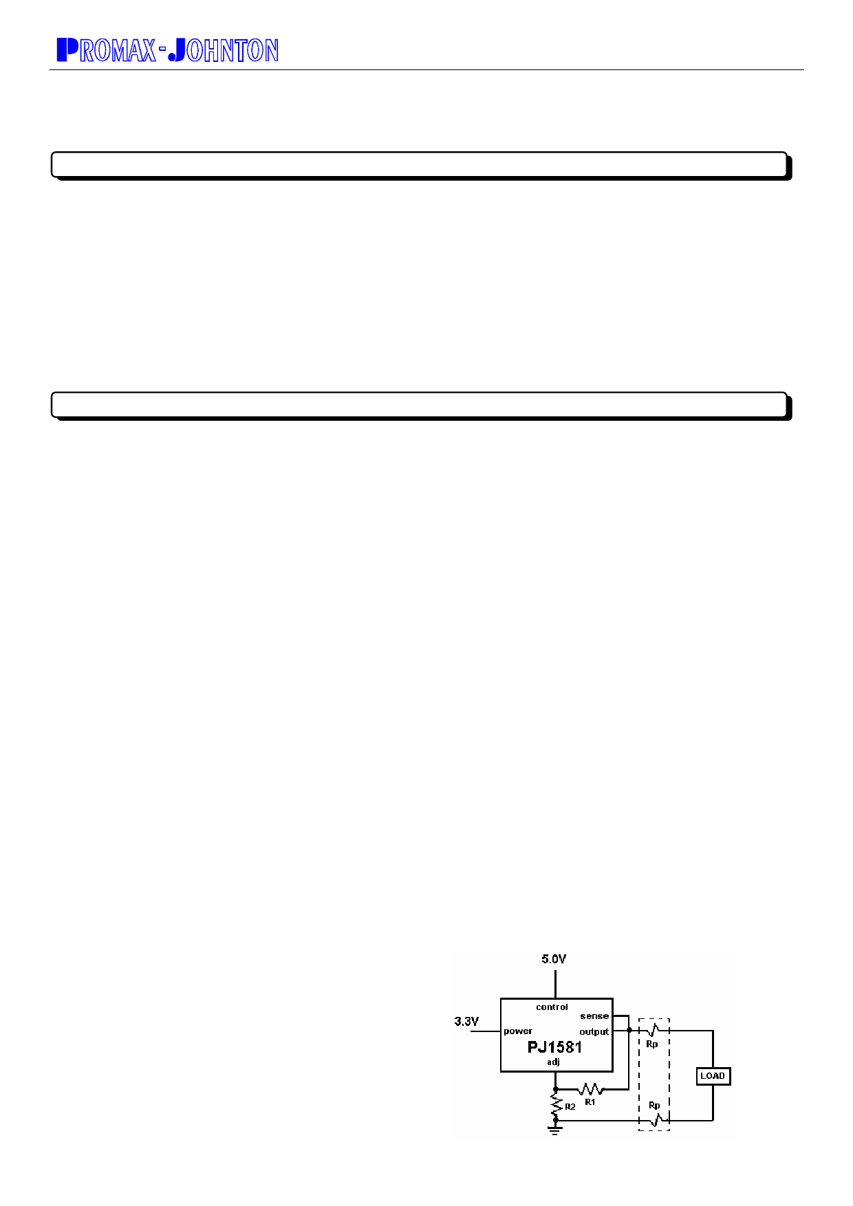
Grounding and Output Sensing
The PJ1581 allows true Kelvin sensing for both the high &
low side of the load. A result the voltage regulation at the load
can be easily optimized. Voltage drops due to parasitic
resistances between the regulator and the load can be placed
inside the regulation loop. The advantages of remote sensing
are illustrated in Figure 1 through 3.
Figure 1 show the device connected as a conventional 3
terminal regulator with the Sense lead connected directly to
the output of the device. Rp is the parasitic resistance of the
connections between the device and the load. Trace A of
Figure 3 illustrates the effect of Rp
Figure 2 show the device connected to take advantage of the
remote sense feature. The Sense Pin and the top of the resistor
divider are connected to the top of the load; the bottom of the
resistor divider is connected to the bottom of the load. The
effect on output regulation can be seen in trace B of Figure 3.
It is important to note that the voltage drops due to Rp are not
eliminated; they will add to the dropout voltage of the
regulator regardless. The PJ1581 can control the voltage at the
load as long as the input-output voltage is greater than the
total of the dropout voltage of the device plus the voltage drop
across Rp
Figure 1. Conventional Load Sensing
3-6
2002.rev.A
Share Link: 