PCA9560 Ver la hoja de datos (PDF) - Philips Electronics
Número de pieza
componentes Descripción
Lista de partido
PCA9560 Datasheet PDF : 17 Pages
| |||
Philips Semiconductors
Dual 5-bit multiplexed 1-bit latched
I2C EEPROM DIP switch
Product data
PCA9560
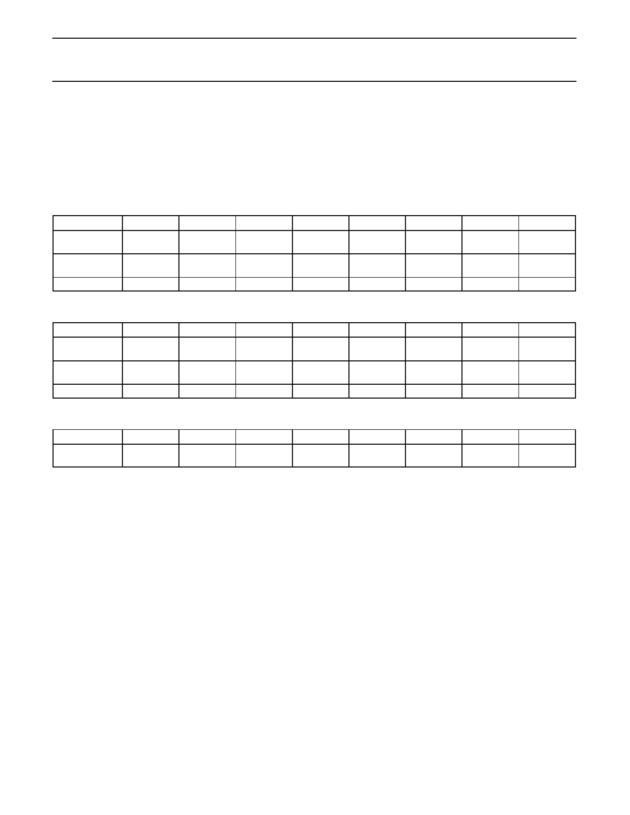
REGISTER DESCRIPTION
If the command byte is an EEPROM address, the next byte sent will be programmed into that EEPROM address on the following STOP
condition, if the WP is logic 0. If more than one byte is sent sequentially, the second byte will be written in the other-volatile register, on the
following STOP condition. If any more data bytes are sent after the second byte, they will not be acknowledged and no bytes will be written to
the non-volatile registers. After a byte is read from or written to the EEPROM, the part automatically points to the next non-volatile register. If the
command code was FFH, the MUX_IN values are sent with the three MSBs padded with zeroes as shown below. If the command codes was
00H, then the non-volatile register 1 is sent, and if the command code was 01H, then the non-volatile register 1 is sent.
EEPROM Byte 0 Register
D7
D6
Write
X
X
Read
0
0
Default
0
0
D5
Non-Muxed
Data
Non-Muxed
Data
0
D4
EEPROM 0
Data E
EEPROM 0
Data E
0
D3
EEPROM 0
Data D
EEPROM 0
Data D
0
D2
EEPROM 0
Data C
EEPROM 0
Data C
0
D1
EEPROM 0
Data B
EEPROM 0
Data B
0
D0
EEPROM 0
Data A
EEPROM 0
Data A
0
EEPROM Byte 1 Register
D7
D6
Write
X
X
Read
0
0
Default
0
0
D5
Non-Muxed
Data
Non-Muxed
Data
0
D4
EEPROM 1
Data E
EEPROM 1
Data E
0
D3
EEPROM 1
Data D
EEPROM 1
Data D
0
D2
EEPROM 1
Data C
EEPROM 1
Data C
0
D1
EEPROM 1
Data B
EEPROM 1
Data B
0
D0
EEPROM 1
Data A
EEPROM 1
Data A
0
MUX_IN Register
D7
D6
D5
D4
D3
D2
D1
D0
Read
0
0
0
MUX_IN
MUX_IN
MUX_IN
MUX_IN
MUX_IN
Data E
Data D
Data C
Data B
Data A
If the command byte is a MUX command byte, any additional data bytes sent after the MUX command code will not be acknowledged. If the
read/write bit in the address is a logic 1, then a read operation follows and the data sent out depends on the previously stored command code.
The MUX_SELECT_1 pin can function as the over-ride pin as on the PCA9559 if the non-volatile register 1 is left at all 0s.
The NON_MUXED_OUT pin is a latched output. It is latched when MUX_SELECT_0 = 1. It is transparent when the MUX_SELECT_0 = 0. The
data sent out on the NON_MUXED_OUT output is the 6th most significant bit of the non-volatile register. Whether this comes from the
non-volatile register 0 or non-volatile register 1 depends on the command code or the external mux-select pins.
After a valid I2C write operation to the EEPROM, the part cannot be addressed via the I2C for 3.6 ms. If the part is addressed prior to this time,
the part will not acknowledge its address.
NOTE:
1. To ensure data integrity, the non-volatile register must be internally write protected when VDD to the I2C bus is powered down or VDD to the
component is dropped below normal operating levels.
2003 Jun 27
5
Share Link: 