PCA9564BS Ver la hoja de datos (PDF) - NXP Semiconductors.
Número de pieza
componentes Descripción
Lista de partido
PCA9564BS Datasheet PDF : 32 Pages
| |||
Philips Semiconductors
Parallel bus to I2C-bus controller
Product data sheet
PCA9564
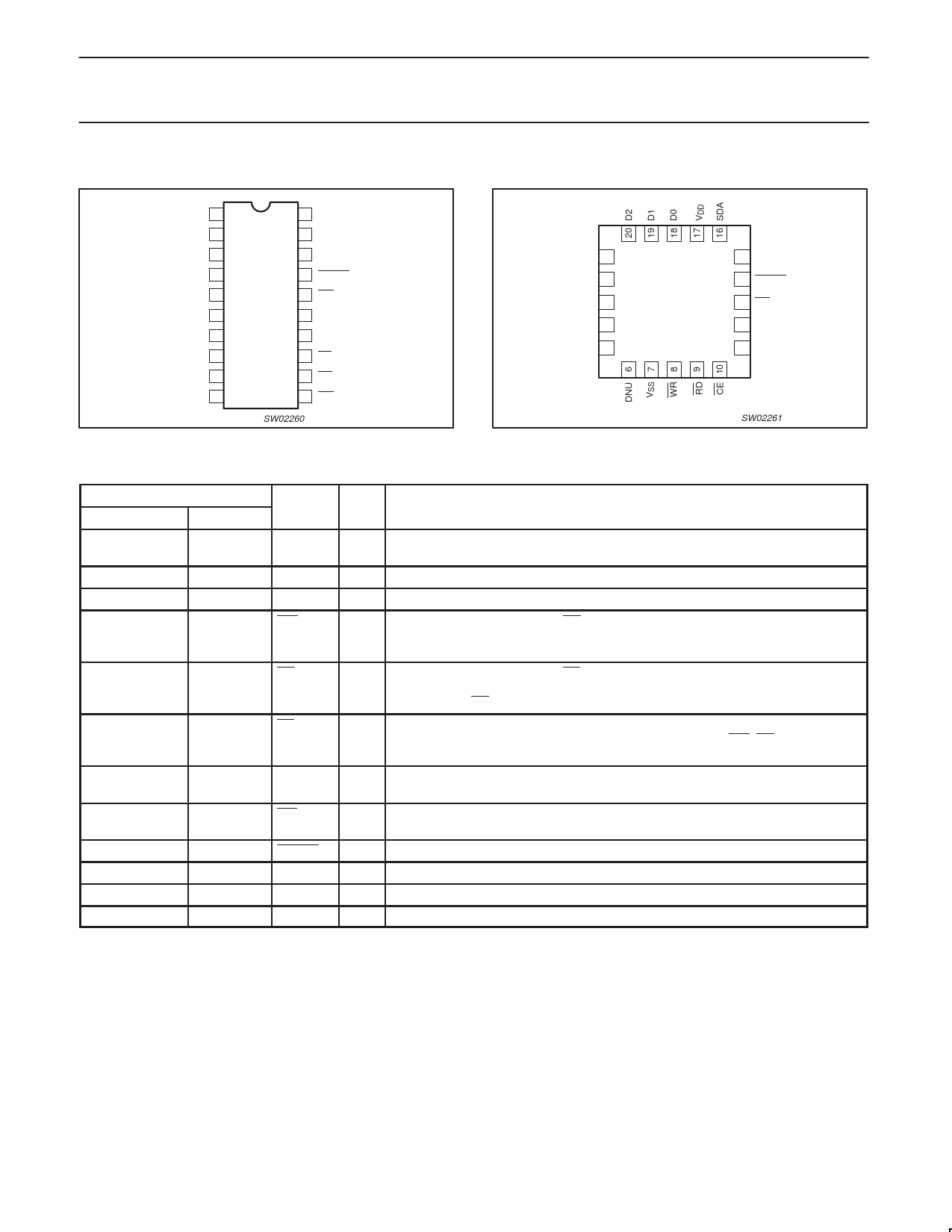
PIN CONFIGURATION — DIP, SO, TSSOP
D0 1
D1 2
D2 3
D3 4
D4 5
D5 6
D6 7
D7 8
DNU 9
VSS 10
20 VDD
19 SDA
18 SCL
17 RESET
16 INT
15 A1
14 A0
13 CE
12 RD
11 WR
SW02260
PIN CONFIGURATION — HVQFN
D3 1
D4 2
D5 3
D6 4
D7 5
TOP VIEW
15 SCL
14 RESET
13 INT
12 A1
11 A0
SW02261
PIN DESCRIPTION
PIN NUMBER
DIP, SO, TSSOP HVQFN
PIN
SYMBOL TYPE
NAME AND FUNCTION
1, 2, 3, 4,
5, 6, 7, 8
1, 2, 3, 4, 5, D0–D7 I/O Data Bus: Bi-directional 3-State data bus used to transfer commands, data and
18, 19, 20
status between the controller and the CPU. D0 is the least significant bit.
9
6
DNU
Do not use: must be left floating (pulled LOW internally)
10
71
VSS
Pwr Ground
11
8
WR
I
Write Strobe: When LOW and CE is also LOW, the contents of the data bus is
loaded into the addressed register. The transfer occurs on the rising edge of the
signal.
12
9
RD
I
Read Strobe: When LOW and CE is also LOW, causes the contents of the
addressed register to be presented on the data bus. The read cycle begins on the
falling edge of RD.
13
10
CE
I
Chip Enable: Active-LOW input signal. When LOW, data transfers between the CPU
and the controller are enabled on D0–D7 as controlled by the WR, RD and A0–A1
inputs. When HIGH, places the D0–D7 lines in the 3-State condition.
14, 15
11, 12 A0, A1 I
Address Inputs: Selects the controller internal registers and ports for read/write
operations.
16
13
INT
O
Interrupt Request: Active-LOW, open-drain, output. This pin requires a pull-up
device.
17
14
RESET I
Reset: A LOW level clears internal registers resets the I2C state machine.
18
15
SCL
I/O I2C-bus serial clock input/output (open-drain).
19
16
SDA
I/O I2C-bus serial data input/output (open-drain).
20
17
VDD
Pwr Power Supply: 2.3 to 3.6 V
NOTES:
1. HVQFN package die supply ground is connected to both VSS pin and exposed center pad. VSS pin must be connected to supply ground for
proper device operation. For enhanced thermal, electrical, and board level performance, the exposed pad needs to be soldered to the board
using a corresponding thermal pad on the board and for proper heat conduction through the board, thermal vias need to be incorporated in
the PCB in the thermal pad region.
2006 Sep 01
3
Share Link: 