PCK2021DGG Ver la hoja de datos (PDF) - Philips Electronics
Número de pieza
componentes Descripción
Lista de partido
PCK2021DGG Datasheet PDF : 15 Pages
| |||
Philips Semiconductors
CK00 (100/133 MHz) spread spectrum differential
system clock generator
Product data
PCK2021
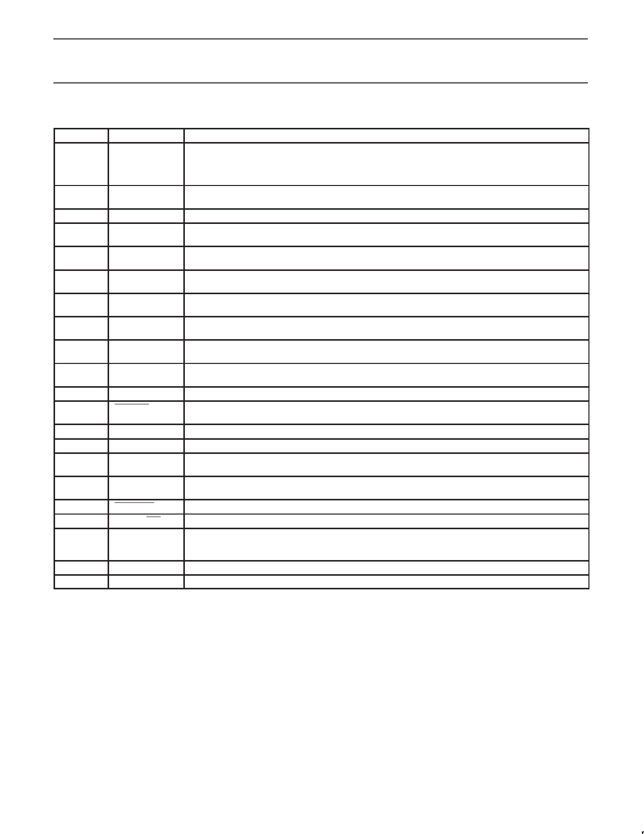
PIN DESCRIPTION
PIN(S)
SYMBOL
1, 2, 8, 9, VDD
12, 18, 24,
25, 31, 37,
40
3, 4
48M_0/SELA
48M_1/SELB
6
3V66
10, 11
HCLK0
HCLKB0
13, 14
HCLK1
HCLKB1
16, 17
HCLK2
HCLKB2
47, 48
PCI0
PCI1
39, 38
HCLK3
HCLKB3
36, 35
HCLK4
HCLKB4
33, 32
HCLK5
HCLKB5
19
REF
20
SPREAD
22
XIN
23
XOUT
26
IREF
29, 30
41
45
5, 7, 15,
21, 27, 28,
34, 46
43
42
MULTSEL0
MULTSEL1
PWRDWN
SEL133/100
VSS
VDDA
VSSA
FUNCTION
3.3 V power supply
Pins 9, 12, and 18 supply host output pairs 0, 1, and 2.
Pins 37 and 40 supply host output pairs 3, 4, and 5.
3.3 V fixed 48 MHz clock outputs. During power-up pins function as latched inputs that enable SELA and
SELB prior to the pins being used for output of 3 V at 48 MHz. Part must be clocked to latch data in.
66 MHz clock: 66 MHZ reference clock
Host output pair 0
Host output pair 1
Host output pair 2
33 MHz clocks: 33 MHz reference clocks
Host output pair 3
Host output pair 4
Host output pair 5
3.3 V fixed 14.318 MHz output
Enables spread spectrum mode when held LOW on differential host outputs, 3V66 and PCI clocks.
Asserts LOW.
Crystal input
Crystal output
This pin controls the reference current for the host pairs. This pin requires a fixed precision resistor tied to
ground in order to establish the correct current.
Select input pin used to control the scaling of the HCLK and HCLKB output current.
Device enters power-down mode when held LOW. Asserts LOW.
Select input pin for enabling 133 MHz or 100 MHz CPU outputs
Ground
3.3 V power supply for analog circuits
Ground for analog circuits
2001 Oct 11
3
Share Link: 