4235 Ver la hoja de datos (PDF) - Peregrine Semiconductor Corp.
Número de pieza
componentes Descripción
Lista de partido
4235 Datasheet PDF : 8 Pages
| |||
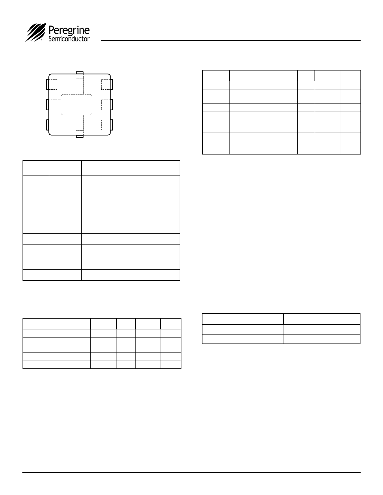
Figure 3. Pin Configuration
RF2 1
GND 2
Exposed Solder
Pad - Shorted
to Pin 2
(bottom side)
RF1 3
6 RFC
5 CTRL
4 VDD
Table 2. Pin Descriptions
Pin
Pin
No.
Name
Description
1
RF2
RF2 port.1
2
GND
Ground Connection. Traces should be
physically short and connected to the
ground plane. This pin is connected to
the exposed solder pad that also must
be soldered to the ground plane for best
performance.
3
RF1
RF1 port.1
4
VDD
Nominal 3 V supply connection.
5
CTRL
CMOS or TTL logic level:
High = RFC to RF1 signal path
Low = RFC to RF2 signal path
6
RFC
Common RF port for switch.1
Notes: 1. All RF pins must be DC blocked with an external series
capacitor or held at 0 VDC.
Table 3. DC Electrical Specifications
Parameter
VDD Power Supply Voltage
IDD Power Supply Current
(VDD = 3V, VCNTL = 3V)
Control Voltage High
Control Voltage Low
Min
2.7
0.7xVDD
Typ
3.0
250
Max
3.3
Units
V
500
nA
V
0.3xVDD
V
PE4235
Product Specification
Table 4. Absolute Maximum Ratings
Symbol Parameter/Conditions Min Max Units
VDD
Power Supply Voltage
VI
Voltage on any input
except for CTRL pin
-0.3
4.0
V
-0.3 VDD + 0.3 V
VCTRL Voltage on CTRL pin
5
V
TST
Storage temperature range -65
150
°C
TOP
Operating temperature
range
-40
85
°C
PIN
Input power (50 Ω)
19
dBm
VESD
ESD Voltage (Human Body
Model)
200
V
Absolute Maximum Ratings are those values
listed in the above table. Exceeding these values
may cause permanent device damage.
Functional operation should be restricted to the
limits in the DC Electrical Specifications table.
Exposure to absolute maximum ratings for
extended periods may affect device reliability.
Control Logic Input
The control logic input pin (CTRL) is typically
driven by a 3-volt CMOS logic level signal. For
flexibility to support systems that have 5-volt
control logic drivers, the control logic input has
been designed to handle a standard 5-volt TTL
control signal. This TTL control signal input must
not exceed 5-volts or damage to the switch could
result.
Table 5. Control Logic Truth Table
Control Voltage
Signal Path
CTRL = CMOS or TTL High
RFC to RF1
CTRL = CMOS or TTL Low
RFC to RF2
Electrostatic Discharge (ESD) Precautions
When handling this UltraCMOS™ device, observe
the same precautions that you would use with
other ESD-sensitive devices. Although this device
contains circuitry to protect it from damage due to
ESD, precautions should be taken to avoid
exceeding the rating specified in Table 4.
Latch-Up Avoidance
Unlike conventional CMOS devices, UltraCMOS™
devices are immune to latch-up.
©2005 Peregrine Semiconductor Corp. All rights reserved.
Page 2 of 8
Document No. 70-0069-03 │ UltraCMOS™ RFIC Solutions
Share Link: 