4240 Ver la hoja de datos (PDF) - Peregrine Semiconductor Corp.
Número de pieza
componentes Descripción
Lista de partido
4240 Datasheet PDF : 8 Pages
| |||
PE4240
Product Specification
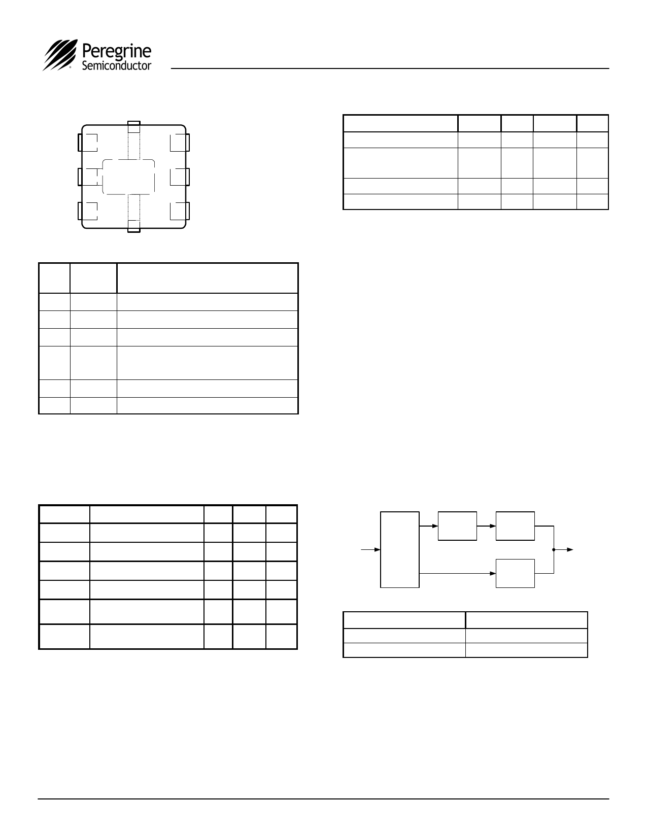
Figure 3. Pin Configuration
RF2 1
GND 2
Exposed Solder
Pad - Shorted
to Pin 2
(bottom side)
RF1 3
6 RFC
5 CTRL
4 VDD
Table 2. Pin Descriptions
Pin Pin
No. Name
1
VDD
2
GND
3
RF1
4
CTRL
5
GND
6
RF2
Description
Nominal 3 V supply connection.1
Ground connection. 3
RF port. 2
CMOS or TTL logic level:
High = RF1 to RF2 signal path
Low = RF1 isolated from RF2
Ground connection. 3
RF port. 2
Notes: 1. A bypass capacitor should be placed as close as possible
to the pin.
2. Both RF pins must be held at 0 VAC or require external DC
blocking capacitors.
3. The exposed pad must be soldered to the ground plane for
proper switch performance.
Table 3. Absolute Maximum Ratings
Symbol Parameter/Condition Min Max Unit
VDD
Power supply voltage
-0.3 4.0
V
VI
Voltage on CTRL input
-0.3 5.5
V
TST
Storage temperature
-65 150 °C
TOP
PIN
VESD
Operating temperature
Input power (50Ω),
CTRL=1/CTRL=0
ESD voltage
(Human Body Model)
-40 85
°C
33/24 dBm
200
V
Absolute Maximum Ratings are those values listed
in the above table. Exceeding these values may
cause permanent device damage. Functional
operation should be restricted to the limits in the DC
Electrical Specifications table. Exposure to absolute
maximum ratings for extended periods may affect
device reliability.
©2006 Peregrine Semiconductor Corp. All rights reserved.
Page 2 of 8
Table 4. DC Electrical Specifications @ 25 °C
Parameter
Min Typ Max Unit
VDD Power Supply
2.7
3.0
3.3
V
IDD Power Supply Current
(VDD = 3V, VCNTL = 3V)
33
40
µA
Control Voltage High
70% VDD
5
V
Control Voltage Low
0
30% VDD V
Electrostatic Discharge (ESD) Precautions
When handling this UltraCMOS™ device, observe
the same precautions that you would use with other
ESD-sensitive devices. Although this device
contains circuitry to protect it from damage due to
ESD, precautions should be taken to avoid
exceeding the rating specified.
Latch-Up Avoidance
Unlike conventional CMOS devices, UltraCMOS™
devices are immune to latch-up.
Device Description
The PE4240 high isolation SPST CATV Switch is
designed to support CATV applications such as
premium channel service connect/disconnect switch
blocks. This function is typically performed by bulky
and expensive mechanical switches. The high
isolation characteristics (>44 dB at 1 GHz, 85 dB
at 5 MHz), high compression point, and an
integrated 75-ohm terminations make the PE4240
an ideal, low cost solution.
Figure 4. Typical Application Block Diagram
CATVin
2-way
Splitter
Premium
Channel
Filter
PE4240
CATVout
PE4240
Table 5. Control Logic Truth Table
Control Voltage (CTRL)
High1
Low
Signal Path (RF1 to RF2)
ON
OFF
Notes: 1. CTRL accepts both CMOS and TTL voltage leads.
The control logic input pin (CTRL) is typically driven
by a 3-volt CMOS logic level signal, and has a
threshold of 50% of VDD. For flexibility to support
systems that have 5-volt control logic drivers, the
control logic input has been designed to handle a 5-
volt logic HIGH signal. (A minimal current will be
sourced out of the VDD pin when the control logic in-
put voltage level exceeds VDD.)
Document No. 70-0067-03 │ UltraCMOS™ RFIC Solutions
Share Link: 